In this video I build a Z8000 (aka Z-8000) Modular Computer.
Note: I’ve started a new section on the blog, titled the Z8000 Modular Computer, with a master index and a page for each board
Why?
I stumbled across the Zilog Z8000 on eBay one day and decided I had to go off and build myself a Z8000 single board computer. I couldn’t fit it all on one board, so I figured I’d made it a two-board computer, then I figured why not add some displays and it because a 3-board computer. Well, next month it’ll probably be a 5-board computer!
Anyhow, the Z8000 was conceived by Zilog back in 1979. It was a 16-bit microprocessor, intended to compute in the 16-bit microcomputer market. It’s contemporaries in the 80s would have been the 8086/8088 and the Motorola 68000. The Z-8000 didn’t quite make it, it was only used in a very few computers. x86 won out, Z-8000 lost.
Build one yourself!
I’ve placed the Gerbers, ROM images, etc., in my github repo linked at the bottom of this page. You can order the pcboards using the gerber files from a place like JLCPCB. You’ll also find PDF format schematics in the github repo, which may be easier to read and zoom than the embedded jpeg schematics on this page.
Zilog Z-8000 Background
The Zilog Z8000 is a 16-bit microprocessor. There’s two versions:
- Z8001. Supports segmented memory, up to 128 segments via the SN0-SN7 pins on the microprocessor. 128 segments with 64 KB of memory per segment allows easy access to 8 MB. An additional SEGT pin allows for the CPU to trap accesses to nonexistent memory. This is a 48 pin DIP IC.
- Z8002. Does not support segmented memory. Omits the SN0-SN7 pins and the SEGT pin. Allows easy access to 64 KB. This is a 40 pin DIP.
I’d suggest you avoid the Z8002 and only use the Z8001, with the segmentation support it’s a much more versatile design. Nevertheless, both CPUs do support two additional ways to get memory, and a clever enough person could probably find a way to get a Z8002 to access 256 KB, or a Z8001 to access 32 MB of memory.
- Split I/D mode. Allows instructions and data to be sent to different pages.
- Normal/System mode. Allows user mode code to be sent to different pages than system code.
Other nice features include a plethora of registers that can easily be combined to form larger registers. For example, the 16-bit R2 and R3 registers can be combined to form a 32-bit RR2. R0/R1/R2/R3 could be combined to form a 64-bit RQ0 register. Memory transfers generally occur 16-bits at a time, with provision to transfer 8-bits at a time for byte operations.
Very few Zilog Z8000 computers were manufactured that used the Z8000. A notable one was the Olivetti M20, which still has some software and other resources up on the web.
Scott’s Z8000 Computer, Modular Design
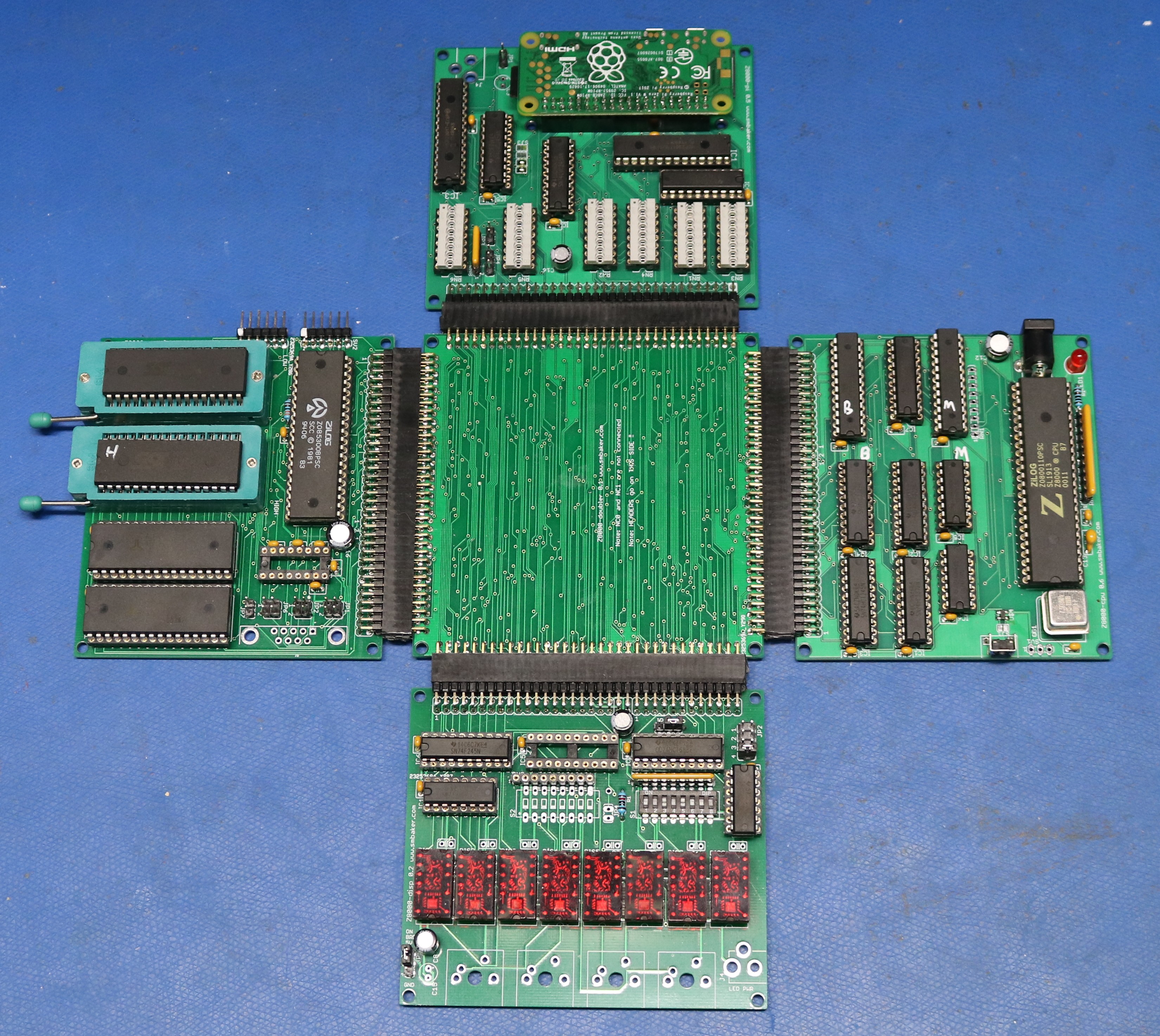
The project is designed into a series of separate modules, with the intention that they could be mixed and matched, and the boards small enough that they can be manufactured at a reasonable cost. A 68-bin BUS connects the boards together, mostly exposing a 16-bit data bus, 20-bit address bus, and some selects for ROM and RAM. The boards are as follows:
- CPU Board. Holds the CPU, Clock, address and data buffers, and bus and memory selection logic.
- Memory and Serial Board. 1 MB of Flash, 1 MB of RAM, and two serial ports using a Z8530 SCC.
- Display Board. Eight TIL311 displays for debugging info, with some provision for input switches and buttons
Schematics
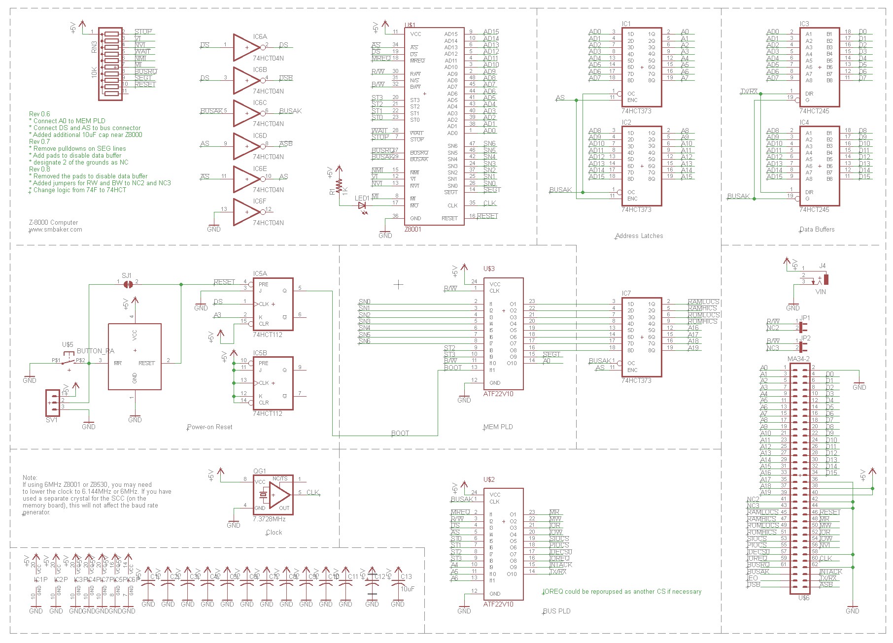
The CPU board uses 74F373 octal latches to latch addresses off the AD bus onto the A bus. The latch occurs on the edge of AS, and an inverter is used to get the appropriate edge. 74F245 transceivers are used for the data bus. The data bus can be live all the time, but it needs to have the direct set appropriately, and this is handled by the TX/~RX pin to the the 245s, which comes from the PLD devices.
The Memory PLD is an ATF22V10C programmable logic device that is used to do memory addressing. See my github repo for the PLD listing. This handles decoding of the segment registers, together with the state pins, and the Byte/Word control line to select the appropriate RAM/ROM ics and to set the upper address bits (A16-A19). Using a PLD allows the segments to be easily reconfigured by the designer, and implement exotic schemes such as separate instruction and data segments. The PLD makes a number of segments available and the listing will indicate which is which.
The Bus PLD is another ATF22V10C. It’s job is primarily to decode the signals necessary to generate IOR, IOW (IO read and Write), and MEMR, MEMW (Memory Read and Write). Again, the PLD listing will explain exactly how this is done. It also generates a few chip selects for common peripherals.
Boot is handled using a flip-flop scheme borrowed from the Olivetti M20. When reset, the Z8000 will read the following:
- FCW from address 00:0002
- Segment from address 00:0004
- Offset from address 00:0006
Then it’ll jump to that segment:offset and begin executing. The boot flip-flop on reset will assert a BOOT signal. The Memory PLD when BOOT is asserted will map the last bank (0x1F) of the Flash into segment 0. This causes the initialization vector to be read from Flash. As soon as A3 becomes positive, the flipflop will deassert the BOOT signal and memory addressing returns to normal (RAM at Segment 0). It’s entirely possible that a simpler scheme could be used, for example leaving the Flash at segment 0 and telling CP/M to use segments other than 0. However, the Olivetti approach seemed elegant and flexible.
A MAX811 IC may optionally be added to handle power-on reset. Without the MAX811, the CPU will sit there like a lump of coal until someone manually presses the rest button.
The LED is attached to the MO line on the CPU that was intended by Zilog for machine-to-machine communication. The “MSET” instruction with light the LED, and “MRES” will extinguish it. I have created the binaries LEDON.Z8K and LEDOFF.Z8K so that this can be done by the user.
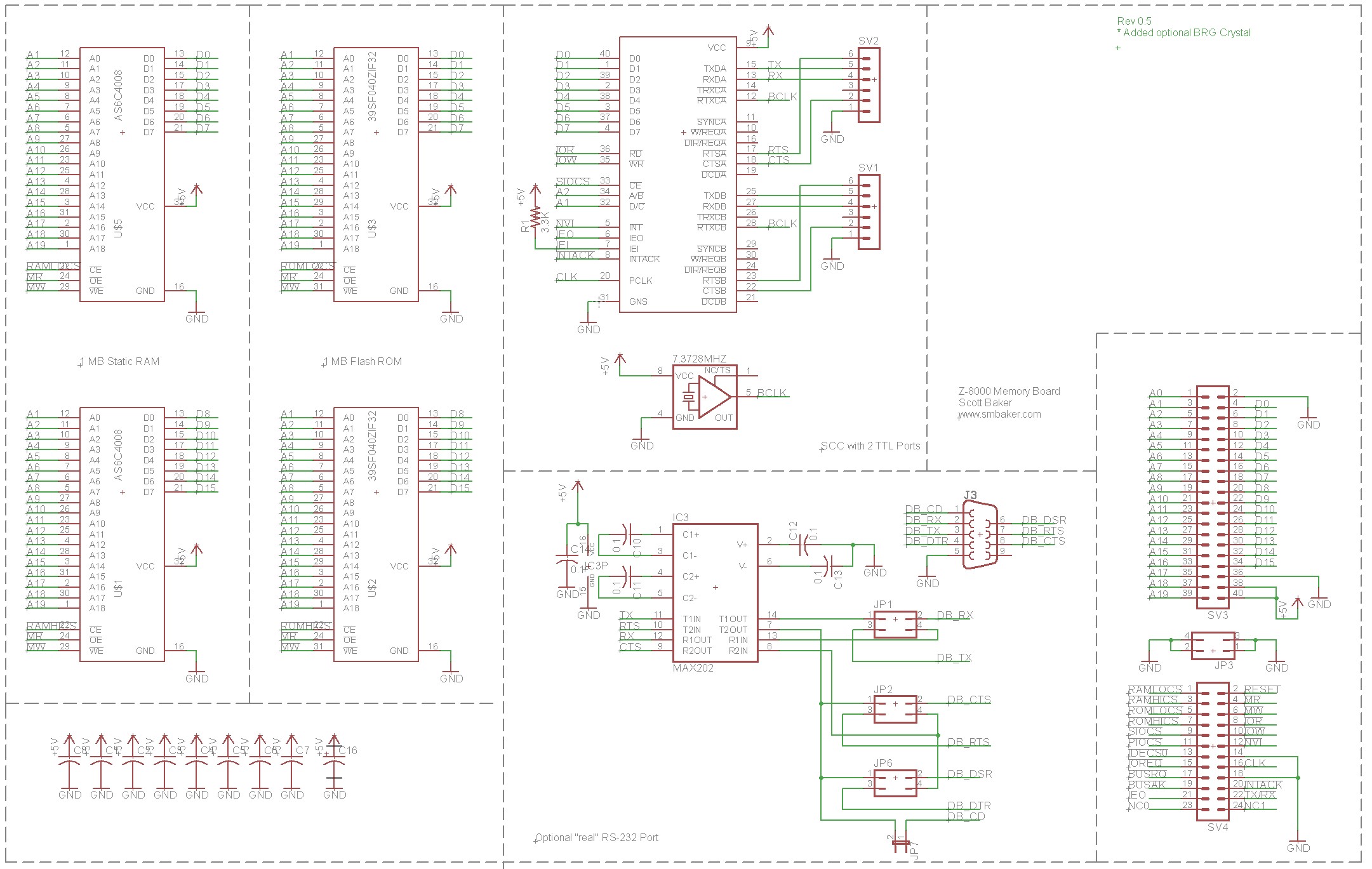
The memory board uses two AS6C4008 SRAM chips for RAM, and two 39SF040 Flash memories for ROM. These are split into low (D0-D7) and high (D8-D15) on the data bus as appropriate. The RAM and ROM are selected by select lines that come from the CPU board.
Also on this board is a Z8530 SCC for serial IO. The SCC is wired to a pair of 6-pin headers than can be used with typical FTDI USB-to-TTL cables. A MAX202 is optionally provided to enable a physical DB-9 serial port for the RS-232 purists out there.
A separate oscillator is provided for the SCC. This allows the baud rate generator in the SCC to be decoupled from the oscillator that the CPU runs at. This means that you can play around with different CPU oscillators (for example, overclocking) without affecting the baud rate generator. There is a build-time software option (see common/board.s) to use the CPU oscillator for the BRG, thus affording you the option to save $$ on oscillators, but the drawback of this approach is the need to use a specific CPU oscillator, 7.3728 MHz.
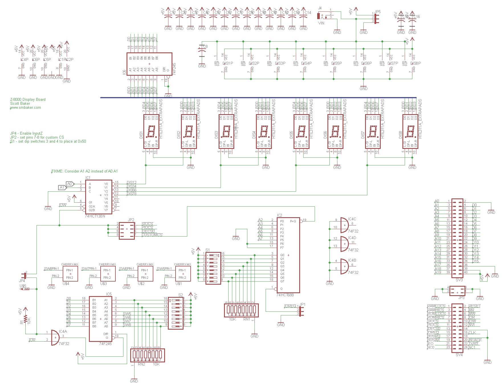
The display board uses TIL311 displays. These displays each take a 4-bit value and display a single hex digit. Eight displays allow four bytes to be displayed. The display board can be jumpered to display either the ports (SIO, PIO, or IDE) from the CPU board, or they can use a custom port selected by dip switches on a 74HCT688., In my configuration, I set the dip switches to place the display board at ports 0x50 – 0x53.
The display board also includes an input transciever than can allow a bank of dipswitches to be read by a user program. It’s my intention to use those dip switches to enable the bootloader to boot different functions. Four Cherry MX footprints are wired in parallel with four of the dip switches to enable momentary buttons. The input logic is optional, and I have not implemented it in the original video.
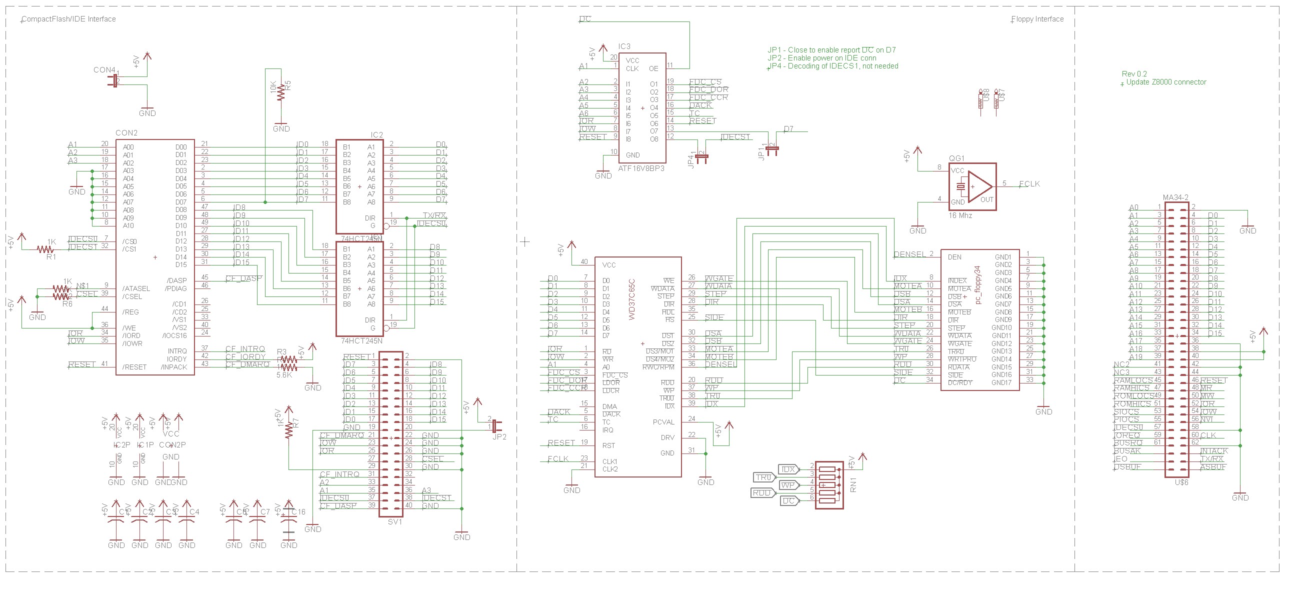
The CompactFlash and Floppy board includes two independent circuits. The first is the CompactFlash/IDE interface. This is relatively simply connected to the bus using a couple of 74HCT245 buffers. The buffers aren’t strictly necessary, but I did notice on one of my IBM PC CF cards that misbehaving compactflash devices could load the bus and make the system unreliable. So I added those buffers here as a safeguard. The chip select for the compactflash is derived from the CPU board.
The other circuit is a floppy controller, based on the WD37C65 floppy controller IC. Its chip selected is derived from an onboard PLD that handles the IO address decoding. The floppy controller circuit has not been tested yet, nor have I updated the BIOS to support the floppy controller yet.
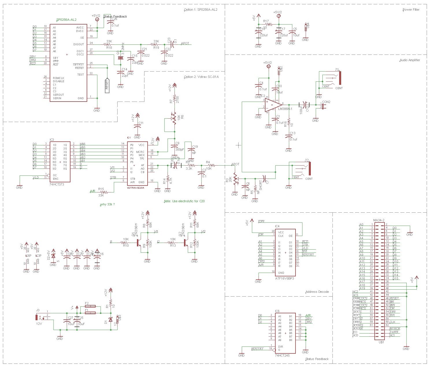
I usually implement a speech synthesizer for my retrocomputer projects, and the Z8000 / CPM-8000 project is no exception, though in this case you get a two for one deal. The speech board is designed to take either a SP0256A-AL2 speech synthesizer of a Votrax SC-01A. So far I have only tested it with the SP0256A-AL2, not with the Votrax, which is somewhat rarer.
The IO decoding for the speech board uses yet another PLD, this time an ATF16V8B. Populate either the SP0256A-AL2 or the SC-01A and their associated support, not both. There’s a latch sitting in front of the data lines to the SC-01A, which is not strictly necessary, but I’m somewhat protective of my excessively rare speech synthesis ICs. The latch is necessary to hold the SC-01A’s inflection pin state, so we needed a latch anyway. The SC-01A needs an additional +12V supply.
The SP0256A-AL2 is easier and it’s cheaper, but it doesn’t sound as good. It does not require the additional +12V supply.
BOM
Bill of materials, approximate — consult the schematics to double-check.
| Symbol | Qty | Part Number | Description |
| (common) | |||
| many | Female double-row 2×40 right angle headers (cur to size) | ||
| many | Male double-row 2×40 right-angle headers (cut to size) | ||
| many | IC sockets, 14-pin, 16-pin, 20-pin, 24-pin, 32-pin, 40-pin, 48-pin, and some 32-ZIFs | ||
| many | 0.1uf | 0.1uF 2.54mm monolithic ceramics | |
| many | straight 2.54mm dupont-style headers (cut to size) | ||
| many | right-angle 2.54mm dupont-style headers (cut to size) | ||
| (cpu board) | |||
| U$1 | 1 | Z0800110PSC | Z8001 CPU |
| U$2, U$3 | 2 | ATF22V10C | Programmable logic device (must program yourself) |
| U$4 | 1 | MAX811MEUS+T | reset circuit, 4.38V threshold |
| U$5 | 1 | right-angle button | |
| IC1, IC2, IC7 | 3 | 74HCT373 | Latch |
| IC3, IC4 | 2 | 74HCT245 | Data Buffer |
| IC5 | 1 | 74HCT112 | Flip-Flop |
| IC6 | 1 | 74HCT04 | Hex Inverter |
| QG1 | 1 | 7.3728 MHz oscillator, or 10 MHz oscillator | |
| R1 | 1 | 10K | 10K Resistor |
| RN3 | 1 | 10K-10 | 10K 11-pin SIP resistor |
| J4 | 1 | barrel jack, for DC-in | |
| C12 | 1 | 100uF | 100uF electrolytic, around 10V |
| (mem board) | |||
| U$1, U$5 | 2 | AS6C4008 | 512Kx8 static RAM |
| U$2, U$3 | 2 | 39SF040 | 512Kx8 flash IC (must program yourself) |
| U$6 | 1 | Z0853008PSC | Z8530 SCC |
| IC3 | 1 | MAX202 | (optional) serial driver, from reputable supplier |
| J3 | 1 | DB9_Female | (optional) DB9 female |
| C16 | 1 | 100uF | 100uF electrolytic, around 10V |
| (display board) | |||
| DIS1-DIS8 | 8 | TIL311A | TIL311A or HIL311A displays, from ebay. Spendy. |
| IC1 | 1 | 74HCT138N | 3-8 decoder |
| IC2 | 1 | 74HCT688 | logic comparator |
| IC4 | 1 | 74HCT32 | |
| IC5, IC6 | 2 | 74HCT245 | data buffer |
| RN1, RN2 | 2 | 10K-8 | 10K 9-pin SIP resistor |
| S1,S2 | 2 | 8-position dip switch | |
| J1 | 1 | (optional) barrel jack, DC-in for displays | |
| C16 | 1 | 100uF | 100uF electrolytic capacitor, around 10V |
| (disk board) | |||
| U$2 | 1 | WD37C65C | (optional) floppy controller |
| QG1 | 1 | 16MHz | (optional) 16MHz oscillator |
| RN1 | 1 | 10K-5 | 10K 6-pin SIP resistor |
| IC1, IC2 | 2 | 74HCT245 | Data Buffer |
| IC3 | 1 | ATF16V8B | Programmable logic device (must program yourself) |
| CON2 | 1 | N7E50-7516PK-20 | compactflash socket |
| R1, R2, R3, R6, R7 | 5 | 1K | 1K resistor |
| R4 | 1 | 5.6K | 5.6K resistor |
| R5 | 1 | 10K | 10K resistor |
| C16 | 1 | 100uF | 100uF electrolytic, around 10V |
Implementation
A minimal implementation requires two boards (CPU and Memory). Note that you cannot simply butt-them together (the pins would be reversed), you need to have some intermediate board between them, As an alternative, you could stack them, like raspberry pi hats.
Most people will probably want to start with a four-board configuration. This gives you room to do CPU, Memory, some storage, and something like the display board or speech synthesizer.
If four board just aren’t enough, then you can go with a 5-board motherboard in the center. The center board keeps getting bigger and bigger as we scale up, but it doesn’t seem to cause any reliability problems.
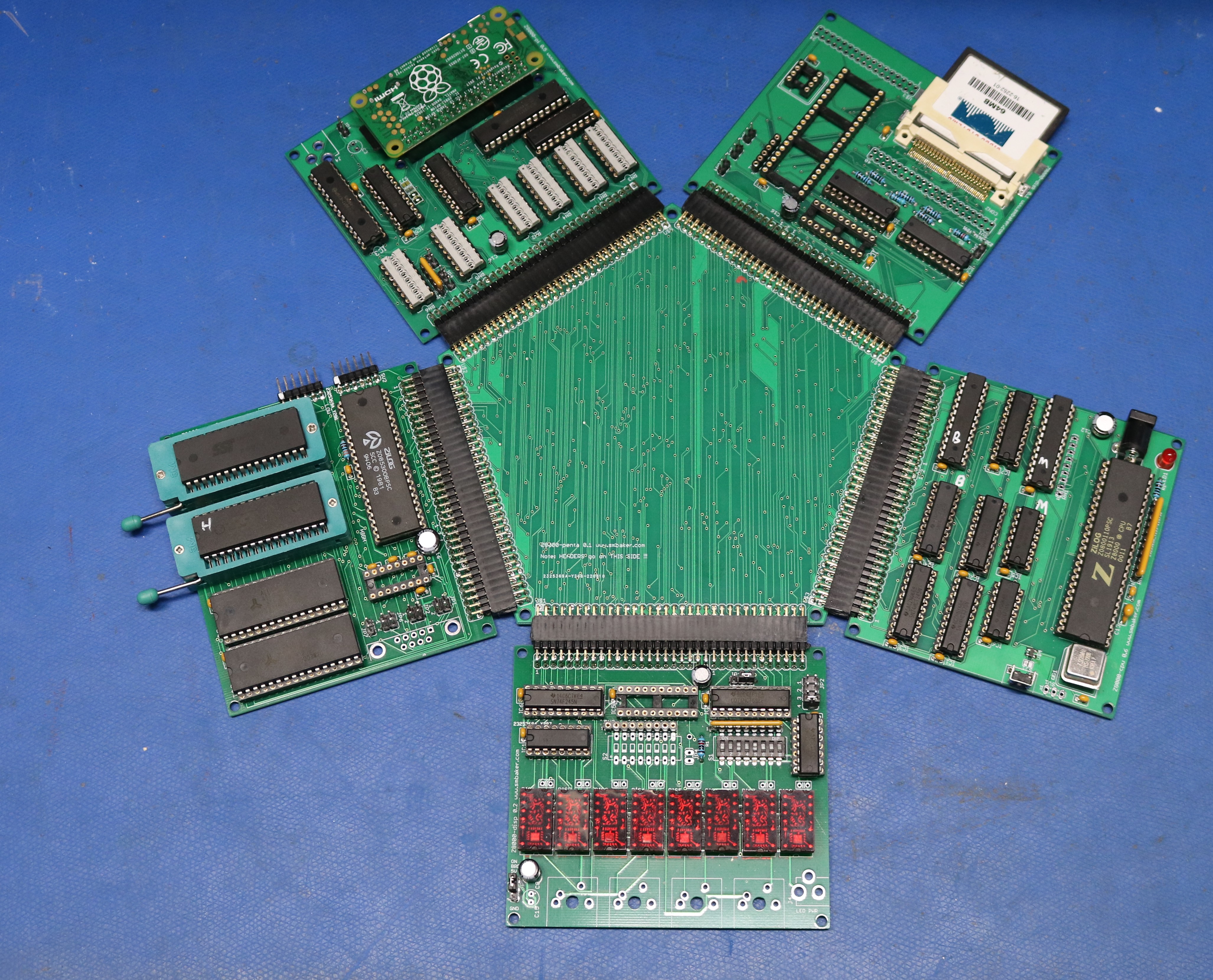
Note that 68-pin headers are either not readily available or prohibitively expensive. If you’re building the clover configuration like I did, just use 80-pin right-angle headers and sockets and cut them down to size. Yes, even the sockets can easily be cut to size with a pair of flush cutters. If you’re building the stacking configuration, then I’d suggest using 40-pin raspberry pi stacking headers, and cut one down to make it fit the 68-pins.
Boot Sequence
I borrowed the boot scheme from the design of the Olivetti M20. The boot sequence is as follows:
- BOOT is asserted by the flip-flop.
- When BOOT is asserted, the Memory PLD maps segment 0 to Flash page 0F. Segment 60 is always mapped to Flash page 0F regardless of BOOT state. This is the last page in flash.
- Page 0F in flash (current mapped to segment 0) contains the initialization vector that the Z-8000 will use to determine where to start executing. The Z-8000 always looks for this in Segment 0.
- The loader’s initialization vector causes the CPU to jump to 60:000C.
- Shortly thereafter, A3 becomes positive, and the boot flip-flop deasserts the BOOT signal. The Memory PLD now maps Segment 0 to RAM page 0. Segment 60 remains mapped to Flash page 0F.
- The loader copies approximately 32KB from 60:0200 to 00:0000. This 32KB contains 4sun5bu’s z8kmon program.
- The loader jumps to 00:0008., starting z8kmon.
- Z8kmon displays a prompt over serial.
- The user presses “B” to boot from flash. z8kmon copies 32KB from Flash page 0, to 03:0000 and then jumps to 03:0000. This 32KB is the start of the flash disk image, and the first thing in the image is the CP/M system code.
- CP/M begins.
CP/M-8000 Notes
CP/M 1.1 is used. 4sun5bu in his github page includes a BIOS that supports IDE and the SCC. I modified this BIOS to use a Flash-based disk. At some point I’ll re-enable the IDE support, and maybe add floppy support.
Memory Segmentation
CP/M-8000 supports (at least) two different modes for loading user programs:
- Nonsegmented shared I/D mode. Both instructions and data are in the same segment and it maps to the same memory page. You can read and write the instruction areas just like any other data. User programs are not aware of multiple segments.
- Nonsegmented split I/D mode. Both instructions and data are in the same segment, but instruction fetches map to a different memory page than data and stack accesses. User programs are not aware of multiple segments. The immediate benefit to this mode is that you gain up to double the space (64K instruction, 64K data) without having to write software that understands segments. A special third segment must be provided, the I-as-D segment, that allows CP/M itself access to the instruction page, so that program text can be loaded by the OS.
CP/M-8000 defines several different memory regions and these regions determine what memory segments are available.
| Region | Name | Segment | Page | Description/Notes |
| 1 | Shared I/D | 1 | 1 | For programs that are shared I/D |
| 2 | Split I/D, Instruction | 11 | 1 | For programs that are split I/D, instructions are here |
| 3 | Split I/D, Data | 11 | 9 | For programs that are split I/D, data is here |
| 4 | Split I/D, I-as-D | 19 | 1 | For programs that are split I/D, segment to use to write to the instruction page. |
| 5 | Special | 0 | 0 | Used by DDT. DDT loads itself here, so as not to interfere with the user program. |
| n/a | CPM System | 3 | 3 | Where the CP/M system (BIOS, etc) is loaded. The system is not replaced by user programs when they are loaded. It is resident all the time. |
Note that it’s up to the designer to choose these segment and page numbers, and the choices above reflect my board. Some programs (ZCC, ED) will load in split I/D mode. Others (PIP, STAT) will load in shared I/D mode. Typically only one user program is loaded at a time, so it’s technically not a problem that regions 1 and 2 are sharing the same page. These region numbers are described in the official CP/M-8000 documentation.
While you could add additional regions, and software could be written to examine the memtbl and make use of additional regions, it’s not clear that any existing CP/M-8000 software does this. Given that fact, the practical memory utilization of CP/M-8000 is 192KB — 64 KB system, 64 KB user instruction, and 64 KB data. The sole exception is DDT, which will allocate an additional 64KB, for a grand total of 256KB.
The ROM Disk
I implemented a ROM disk using the same 39SF040 flash memory that holds the BIOS. Technically this is Flash, but I’ll call it ROM anyway as that’s how we’re using it. 64KB (1 page) of ROM is reserved for the bootloader and monitor. That leaves 960KB for the ROM disk.
The ROM disk is implemented in the Bios. Rather than reading from external storage, it does a simple computation to convert the track and sector number to an offset, and transfers the data from RAM.
The RAM Disk
I also implemented RAM disk using the same AS6C4008 SRAM chips that are used for program and system memory. 256KB are required for the system, and I reserved another 64KB for a hypothetical second page (in case I want to try to make some segmented programs some day). That leaves 705KB for the RAM disk.
It’s implemented almost identically to the ROM disk — reads/writes are diverted to the ram disk code, and data is simply transferred between memory. The RAM disk uses pages 4,5,6,7,8,10,11,12,13,14,15 — page 9 is omitted because it’s part of the Split-I/D scheme.
Hunting the Wumpus!
If you watched the video, you might have noticed that I had some bugs where ED.Z8K and some other tools wouldn’t run. Those turned out to be a problem with memory segmentation for split I-D spaces, which I fixed. Then I managed to find some olivetti disks with wump.z8k on them… and now we have playing games on the Z-8000.
Z8001 Machine Code Monitor Ver.0.3.0
 Modified by Scott Baker (smbaker@smbaker.com) for Scott's Z-8000 Computer
 Press 'B' to boot or 'H' for help
   b
   Boot CP/M from Flash… Jumping to CP/M start
 CP/M-8000 BIOS ver.0.11.smbaker1
  CP/M-8000(tm) Version 1.1 12/19/84
  Copyright (c) 1984, Digital Research Inc.
 A>wump
 Instructions? (y-n) n
 You are in room 19
 Bats nearby
 There are tunnels to 2 16 18
 Move or shoot (m-s) s
 Give list of rooms terminated by 0
 2 16 18 0
 You are in room 19
 Bats nearby
 There are tunnels to 2 16 18
 Move or shoot (m-s)
Tiny Basic
I ported tinybasic-for-arduino to the Z8K. It compiles and build using the zcc compiler that’s part of the CP/M-8000 distribution on the Z8000.
A>tbasic
Z8000 TinyBasic, www.smbaker.com
32606 bytes free.
OK
10 print "scott was here"
20 let a=1
30 let b=2
40 print a+b
run
scott was here
3
OK
Tinybasic is included in the rom disk image, so you too can jump right into writing BASIC programs on your CP/M-8000 computer. While I wouldn’t recommend this particular BASIC for serious programming, I’d use the zcc compiler instead, it is useful for quick demos.
Zork!
I ported the mojozork Z-machine by Ryan C. Gordon to the Z8000. Like tinybasic, I compiled this (after significantly modifying it) right on the Z8000 computer. So now you can play Zork also. It helps to have a few things to do on the computer.
A>zork
z8kzork based on mojozork by Ryan C. Gordon.
modifed for cp/m-8000 by Scott M Baker, www.smbaker.com

ZORK I: The Great Underground Empire
Copyright (c) 1981, 1982, 1983 Infocom, Inc. All rights reserved.
ZORK is a registered trademark of Infocom, Inc.
Revision 88 / Serial number 840726

West of House
You are standing in an open field west of a white house, with a boarded front door.
There is a small mailbox here.

>open mailbox
Opening the small mailbox reveals a leaflet.

>take leaflet
Taken.

>read leaflet
"WELCOME TO ZORK!

ZORK is a game of adventure, danger, and low cunning. In it you will explore some of the most amazing territory ever seen by mortals. No computer should be without one!"
The program takes a single argument that is the name of the game file to load, and it loads zork1.dat by default. With the appropriate data file, it can also play Zork 2, Zork 3, or any other Infocom game that is compatible with version 3 of the z-machine.
Common Problems
- Board does not boot / does not come out of reset. Make sure you’re using a high-quality power cable to supply the board. A poor quality cable may drop as much as a half of a volt. If you’re using the MAX811, it is a voltage-triggered device — too little voltage and it will keep the Z-8000 in reset. If you have less than 4.38V at the pins to the MAX811, it will not leave reset. As an alternative, you can leave the MAX811 out of circuit, solder the nearby solder jumper, and you will have to manually reset the CPU each time you power it on.
- Board is flaky / problematic / crashes often. I found that the logic family matters. When using 74F logic, the same family that 4sun5bu chose, I had flaky performance. Switching to 74HCT resolved the problem entirely. It’s possible that the higher energy consumption of the F chips, together with imperfect PCB routing of the power traces, could have been leading to intermittent issues.
- No output on serial port. Try disconnecting pin 6 (RTS). Some FTDI adapters are buggy and don’t do RTS properly. The CP/M-8000 BIOS is setup to enable CTS/RTS handshake, and if RTS is high instead of low, then output on the serial port will be suspended until RTS is asserted low. Alternatively, this could be disabled in the BIOS (turn off bit5 on register3 in the 8530).
- Floppy Controller board and Video Board won’t work together. Make sure to program the PLDs on the CPU Board as “ATF22V10C (UES)”. This has to do with GAL mode vs PAL mode. Currently thinking is that if you program it in the wrong mode, you will cause the power-down bit to be set, which may cause outputs to be latched at odd times.
Resources
- Scott’s Z8000 repo with PLD files, schematics, code, gerbers, etc.
- 4sun5bu’s Z8001MB project, with information on his project. I used the BIOS and the Monitor from this project, and drew some inspiration from the hardware design.