In this video, I build a bubble memory board for my Heathkit H8:
Purpose / Background
In the short time I’ve owned my H8, I’ve amassed several different storage options:
- H17 floppy controller board by Norberto Collado
- H8-Dual-Compactflash Board by Douglas Miller, Richard Davis, and Norberto Collado
- H8-8MEG-Ramdisk Board
- … and now the H8 Bubble Memory Board!
The most practical of these is the dual compactflash board. It offers plentiful, durable storage that is easily transportable between the H8 computer and your PC. It makes use of commodity parts that are readily available. However, sometimes it’s fun to not be practical!
Bubble memory was a technology of the 1970s, perhaps enduring a slightly longer life cycle in the industrial machinery space, where machinery vibration was particularly problematic for storage deivces like floppy disks or hard disks. Bubble memory makes use of special magnetic patterns deposited on a substrate such as garnet, to be able to migrate magnetic “bubbles” in a loop configuration. You can rotate the bubble you’re interested around the loop and the duplicate it for reading, or you can swap in a different bubble for writing. Magnetic bubble memory is a nonvolatile memory and will preserve its contents on power-off.
Learning about Bubble Memories
I’m not going to go into technical detail on bubble memory here, as other enthusiasts have already done so, and done a better and more thorough job than I probably would have. Here are some useful resources:
- Hackaday Article on Craig Andrews’s SBC-85 Bubble Memory Project
- Craig’s videos, starting with this one: Magnetic Bubble Memory Fundamentals 101. He has at least 3 more, so make sure to watch them all for a thorough understanding.
- Craig’s blog posts, on his website
- Bubble Memory Design Handbook. You can find archived copies of this on the public Internet.
- Application Note AP-187, “MEGABITS TO MEGABYTES: Bubble Memory System Design and Board Layout”. You can also find archived copies of this on the public Internet.
The Bubble Memory Reference Circuit
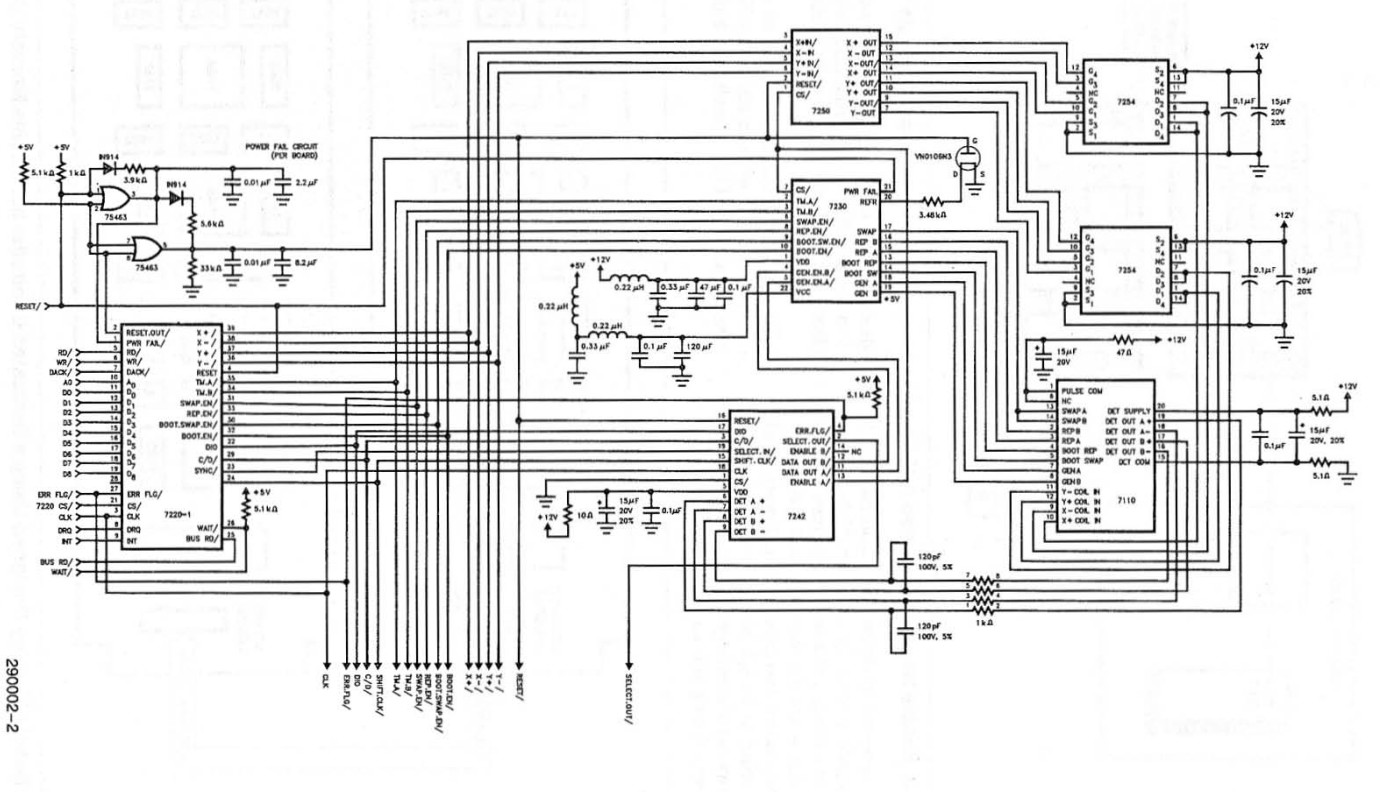
The bubble memory design handbook and the ap187 document tell you everything you need to know to implement the reference circuit, at both the block level:
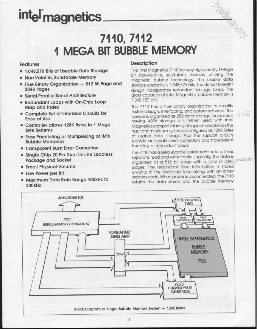
Bubble Memory on the H8
Fortunately, Craig’s SBC-85 design provided me with almost everything I needed to start with. There’s the schematic of his SBC-85 board itself, as well as 8085 assembly code for reading and writing sectors and exercising other commands on the bubble memory controller.
My tasks were the following:
- Interface the bubble memory controller to the H8 Bus
- Write a storage driver for HDOS, so the bubble memory could be used as a disk
- Add support to Douglas Miller’s Newmon monitor for the H8, so that bubble memory could be booted directly.
That’s about a weekend’s worth of tinkering…
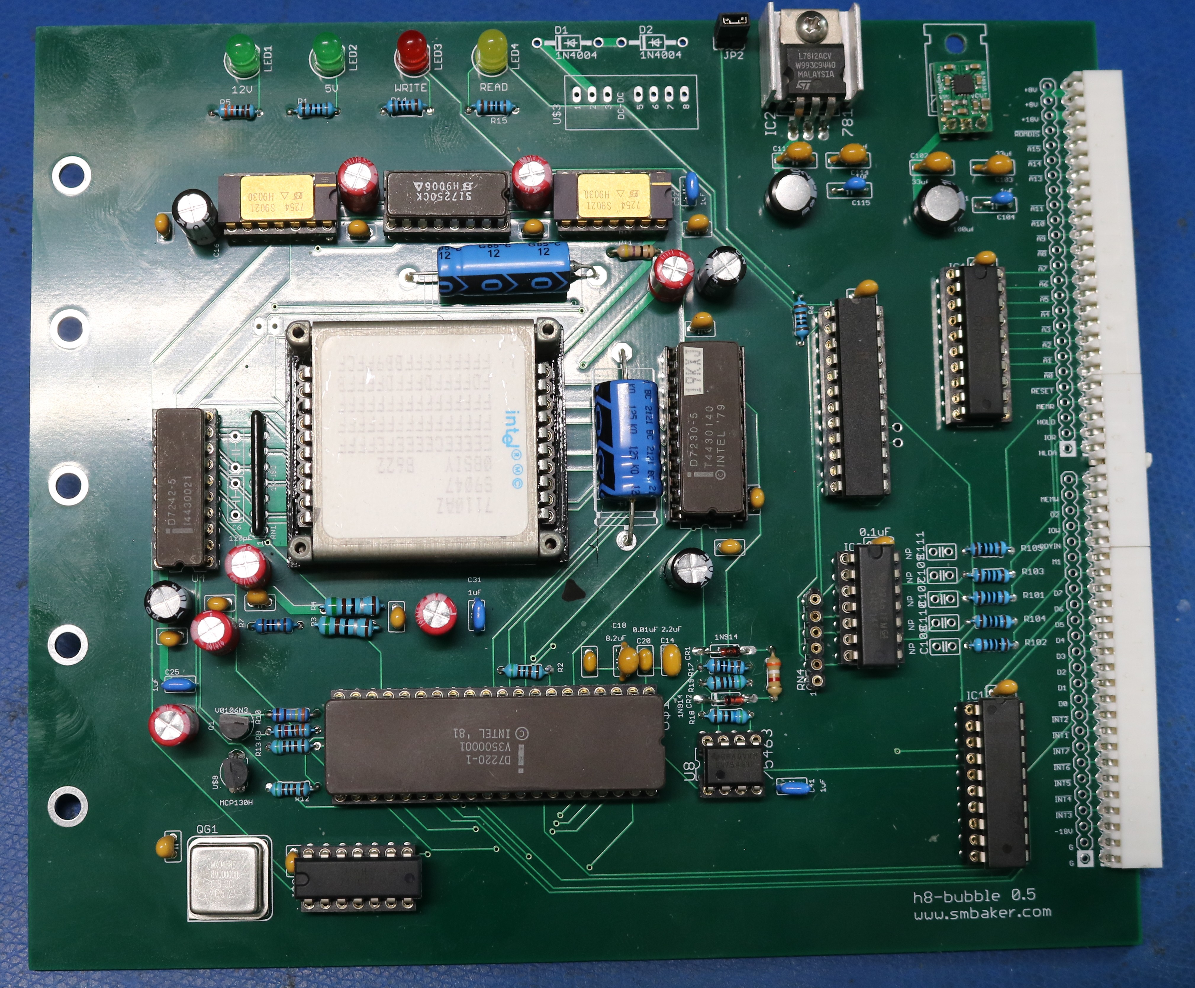
Hardware Design
The full schematics are checked into the github repo [TODO: Check in once revision has been tested]. Interfacing the bubble memory controller is relatively simple:
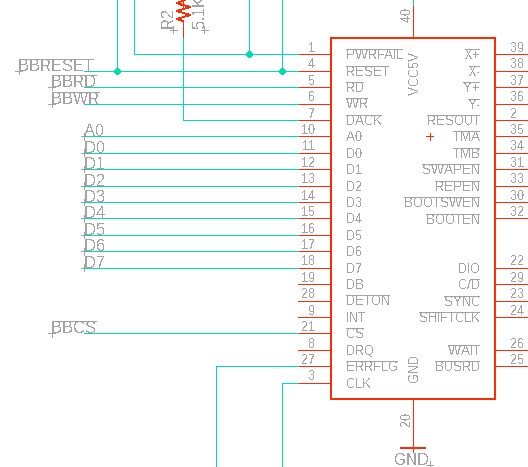
The CPU interface are all of the labeled lines on the left of the schematic. These include
- /BBRESET. The reset signal from the H8 bus.
- /BBRD. An IO read strobe. The H8 bus IOR is suitable once inverted.
- /BBWR. An IO write strobe. The H8 bus IOW is suitable once inverted.
- /BBCS. A chip-select signal. We need to match the lower address bits (A0-A7) to the address we’re interested in.
Here’s how we obtain all those signals:
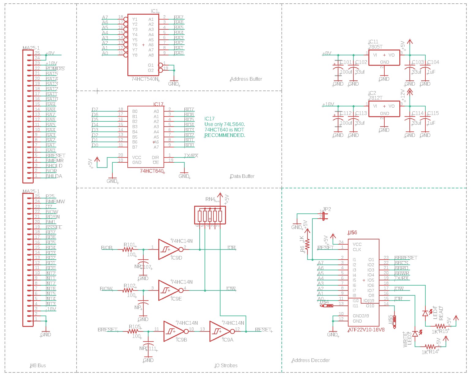
The H8 bus is inverted, so inverting buffers are used for the address bus, the data bus, and the IO strobes. You can see this in the ‘540 and ‘640 ICs. The IO strobes I have used some RC filtering as my H8 tends to have some noise on this lines. The associated resistors and capacitors on BIOR, BIOW, and BRESET can probably be left off (i.e. the resistors wired across with a jumper) if you don’t have such issues.
Address decoding is performed by an ATF22V10/GAL22V10D or an ATF16V8, depending on which part you have handy in your inventory — I will include the PLD code for each of them. /BBCS is driven by decoding the address bits A7..A1. We don’t need to decode the least significant address bit (A0) as that line is connected to the 7220. In addition to address decoding, the PLD also handles driving a couple activity LEDs.
The /IOR, /IOW, and /RESET pass through the PLD directly to /BBRD, /BBWR, and /BBRESET respectively. I plumbed them through the PLD in case I wanted to do something fancy with them, but I did not.
That leaves the TX/RX line, which controls the direction of the ‘640. We use IOR together with the address decoding to determine when to put the ‘640 into the receive direction. If we’re reading from the bubble memory, then we’re receiving to the bus. If we’re writing to the bubble memory, then we’re transmitting from the bus.
I’m not going to reproduce the schematic here in the blog post for the bubble memory circuit itself — you can view the PDF in the github repo, consult the Bubble Memory Guide, or have a look at Craig’s SBC-85 schematic. All of these reproduce essentially the same reference implementation from the official literature.
Hardware Implementation
Here’s a picture of the first prototype:
Software
The software was relatively straightforward to implement using Craig’s SBC-85 code as a baseline. I already had my H8 Ramdisk implementation from my previous blog post on the H8-8MEG board, so I had already learned the necessary steps to write an H8 disk driver. We really needed to just marry the two pieces of code together, so that requests for data from the disk driver were connected to the SBC-85 code for reading and writing blocks. The SBC-85 code handles reads and writes up to approximately 16KB in size. My code from the H8-8MEG board was already designed to break reads and writes into chunks of 16K. This was a straightforward port.
Once that is done, the next step is to write a “readonly” driver. The readonly driver is used in the HDOS boot sector and must with within 512 bytes. You basically throw everything overboard that you can get away with (including in this case some error-checking code) in order to make it fit. The readonly driver is used by HDOS to read the OS and the real (read-write) driver to bootstrap the system.
Finally, we need to update Douglas’s Newmon monitor to support the bubble disk. The monitor reads the first 10 sectors of the disk (which will include the readonly driver) and jumps into it. So it’s really just a matter of dropping the bubble read code in one more time, to read those sectors.
Resources
- Github Repository. Schematics, Gerbers, Software, PLD files, etc. [TODO — Waiting to verify latest board design]