In this post, I create a DRAM board for the Heathkit H8 computer. No video yet, but plenty of text. 😀
Purpose / Motivation
I like boards with rows and rows of DRAM chips. Makes me feel like I’m in the 80s again!
Most of the modern boards for the Heathkit H8 use static RAM. Most of the vintage boards use static RAM as well. There were a few noteworthy boards back in the day that used dynamic RAM, most notably a board by Trionyx. I decided I’d try to invent my own board.
The H8 computer allows several different CPU boards to be used. The H8 originally shipped with an 8080 CPU, but later upgrades included a Z80. In another project, I developed my own 8085 based CPU board. A goal of this project was to ensure that the DRAM board worked with all three of these CPU options, each of which have slightly different memory idiosyncracies.
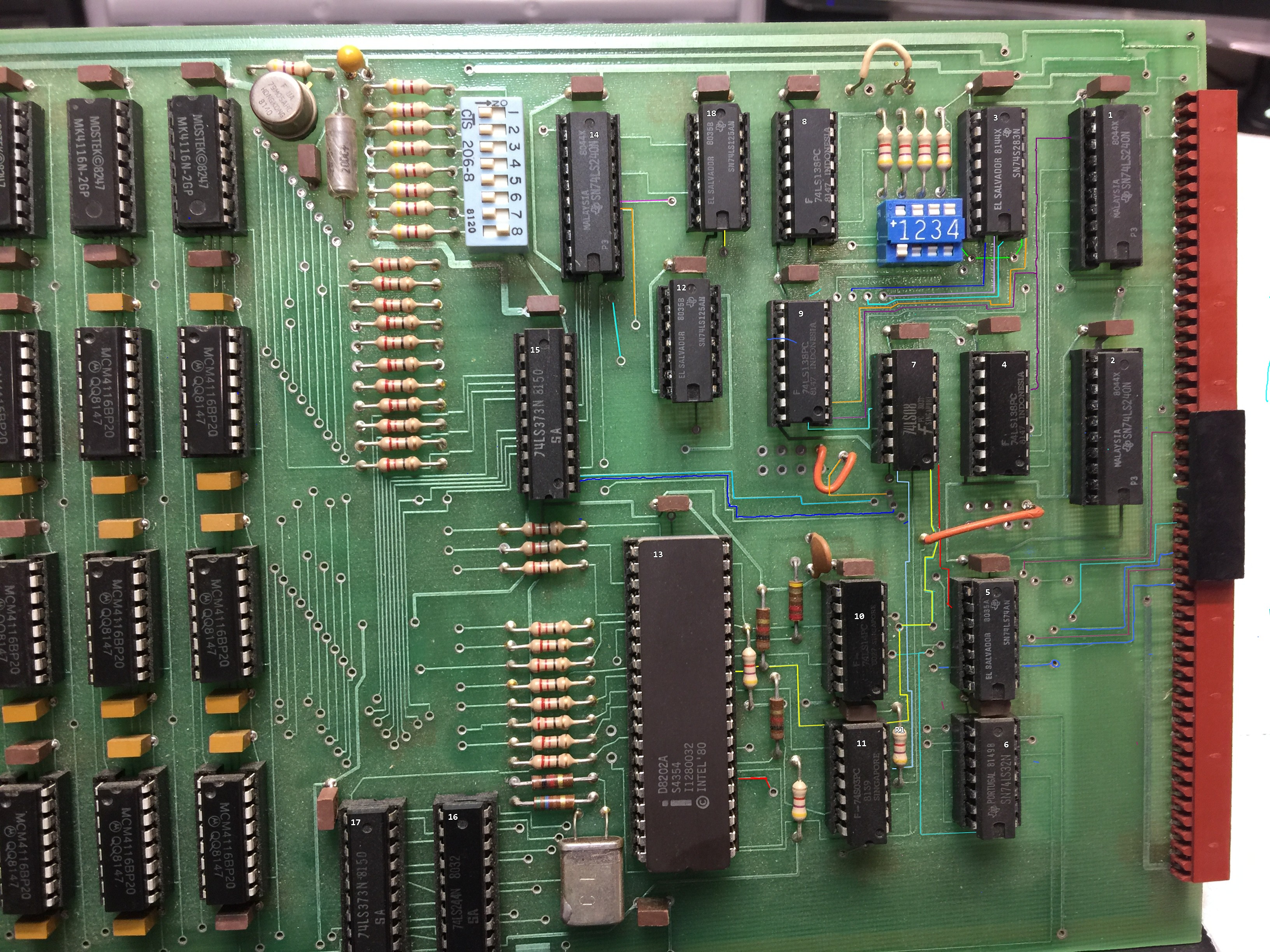
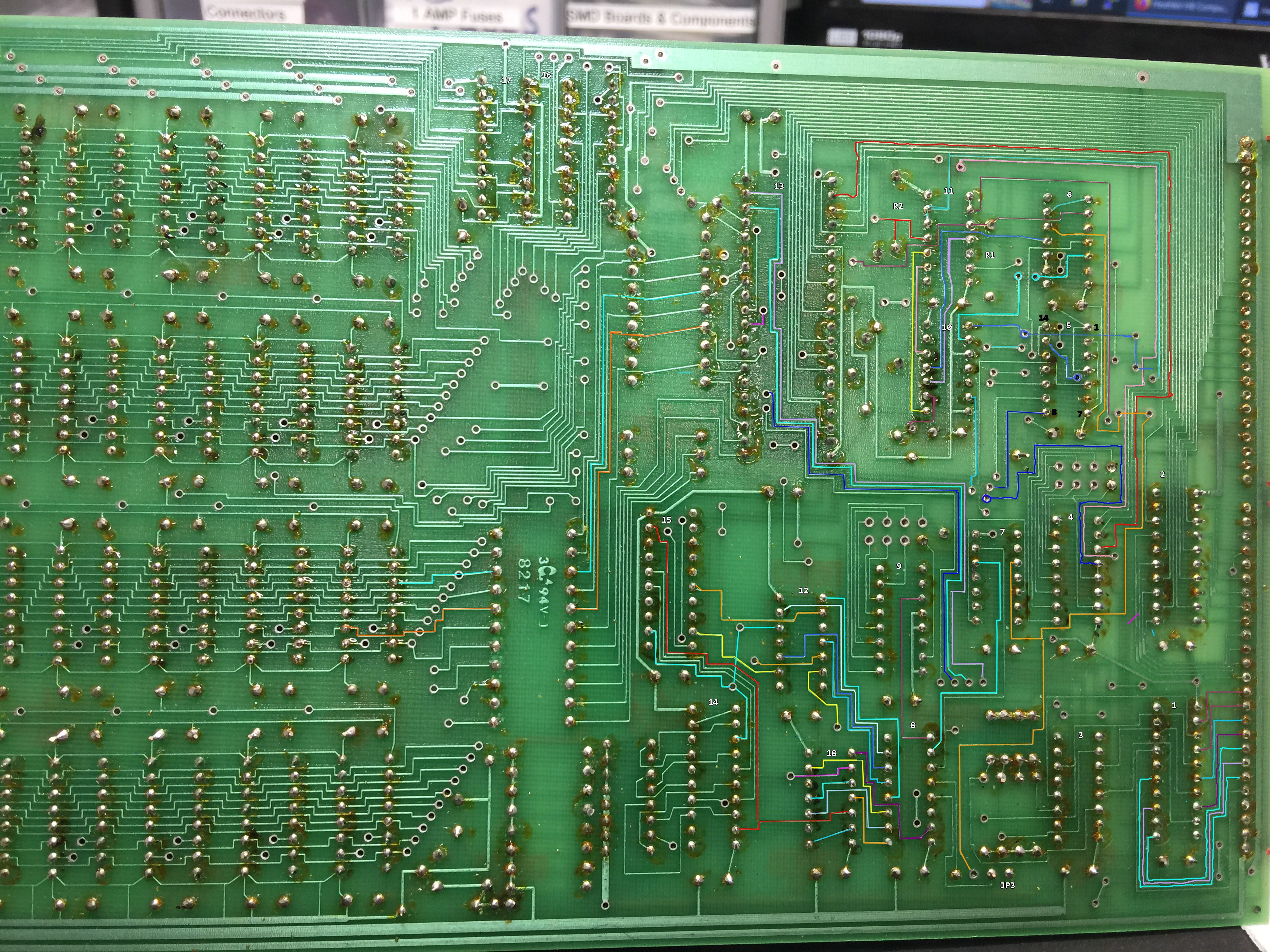
Full schematics and gerber files are present in my github repo. See link near the bottom of this writeup should you wish to build a board. This is an advanced project that may be somewhat challenging for the novice.
Choosing a DRAM controller
I knew from the start of the project that I didn’t want to implement DRAM timing from scratch. DRAM timing is complex, needing to assert RAS, CAS, and Write signals at just the right time, and needing to schedule memory refresh. Unlike static RAM, you can’t just set-it-and-forget-it with DRAM — it needs to be frequently refreshed. A DRAM controller can take care of this timing for you. A couple options presented. The first was the 74S409. The second one I came across was the Intel D8202 and D8203. I read the datasheets and decided to go with the latter.
D8202 and D8203 are similar with a few noteworthy differences. D8202 can only use 16K DRAMs, whereas D8203 can use either 16K or 64K DRAMS. D8203 includes current limiting resistors built in. I decided of the two, to use the D8203.
This should be a piece of cake…
The D8203 datasheet made everything sound oh so simple:
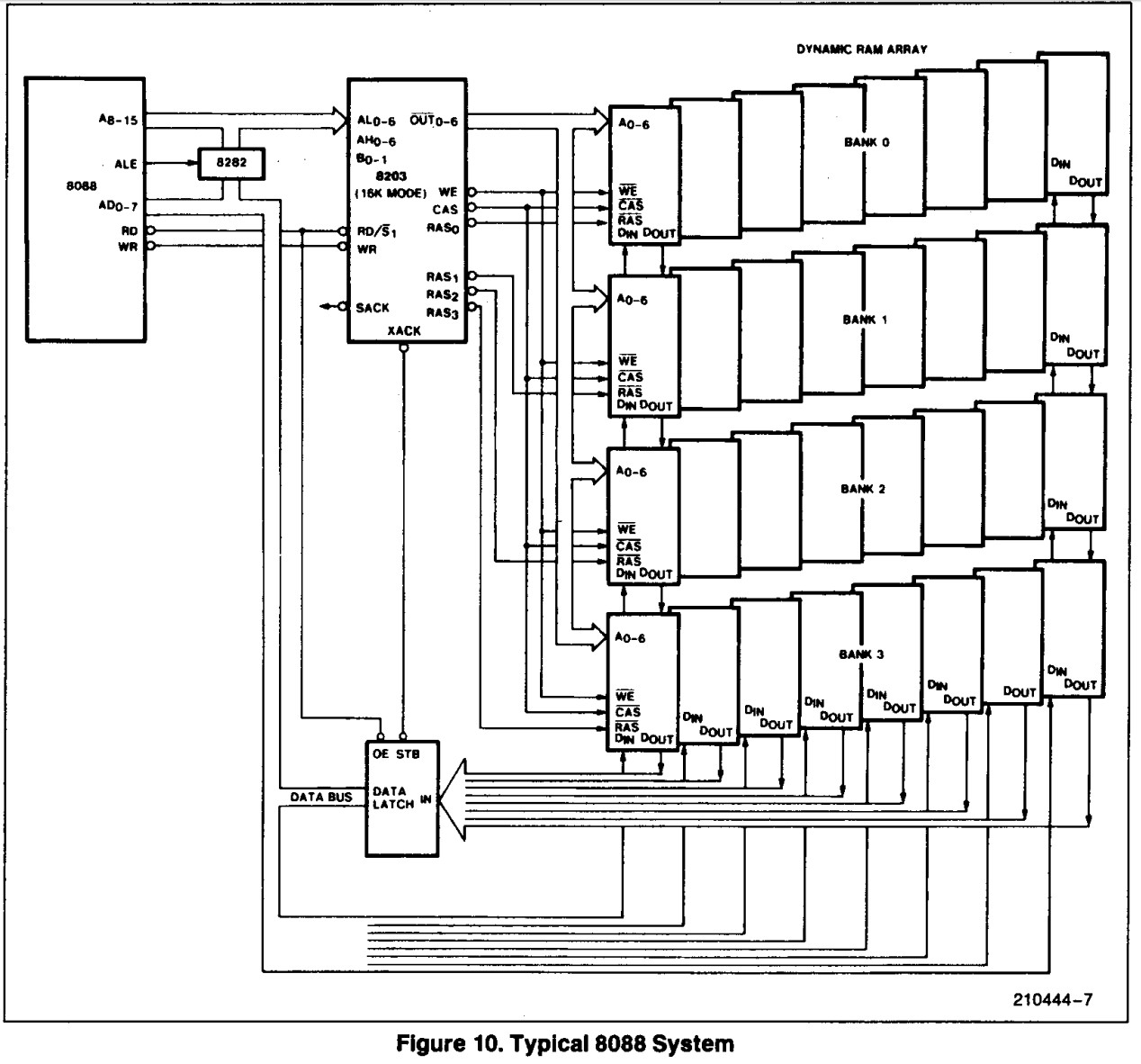
Just the DRAM controller and a latch. I can do that! The D8203 will handle all of my DRAM timing, and even schedule refresh for me. It’ll generate a signal called /XACK that I can use to make the CPU wait while the DRAM is busy refreshing.
As we will soon see, life gets more complicated very quickly.
Failure #1: Assuming /XACK == WAIT
My first prototype use /XACK to generate a wait state based on what I saw in this pictures:
Turns out my interpretation wsn’t how it worked at all. /XACK doesn’t generate wait states. /XACK signals that a transaction is complete. The datasheet is perfectly clear on this, but the above picture might mislead you into trying to take the simple route and just plugging /XACK into your WAIT signal. It doesn’t work that way. Not at all!
In fact, /XACK might not even occur until well after the CPU completes the memory transaction. The DRAM controller could be busy servicing a refresh, and acknowledge the memory transaction relatively late. This led me to the realization that I really wanted my wait state to occur from then time when /RD or /WR was asserted, until the time when /XACK gets asserted.
Failure #2: Realizing that WAIT doesn’t start with /XACK, but ends with /XACK, but still not getting it right.
Fresh off the learnings from Failure #1, I implemented logic that would begin the wait state when /RD or /WR is asserted, and not release it until /XACK is asserted. Here’s what I ended up with in my PLD equations:
MW = BMEMW & !XACK;  /* RD signal to DRAM controller */
MR = BMEMR & !XACK;  /* WR signal to DRAM controller */
LOE = BMEMR & CS;    /* read latch output to bus */
OLATCH = XACK;       /* read latch capture DRAM outputs */


/* This is a tricky mess. When RD or WR occurs, we need to assert
   wait until the corresponding !XACK comes along and is asserted (low)
   and then released (high).
*/

WAIT = (WAIT & XACK) # ((BMEMR#BMEMW) & CS & !TMP);
TMP = ((BMEMR#BMEMW) & CS & XACK) # ((BMEMR#BMEMW) & CS & TMP);
The above wasn’t actually quite right — I was trying to hold WAIT until /XACK was both asserted and released. The DRAM controller won’t release XACK until /RD and /WR is released, so you can also see some logic there to release /MR and /MW.
This almost worked, but would occasionally glitch and wouldn’t quite load HDOS. This HDOS inconsistency turned out to be an entirely different problem, which you can read in a footnote at the tail end of this write-up.
Failure #3: Thinking a flipflop would solve all my troubles
I thought Failure #2 was due to not properly implementing edge triggering, so I reimplemented the PLD WAIT logic with a flipflop. I preset the flipflop on a MEMR or MEMW from the CPU, and I clocked a ‘0’ into the flipflop on /XACK. This was me still thinking I had to wait for /XACK to both assert and release. It really didn’t work any better than failure #2.
Failure #4: The Compupro non-Solution
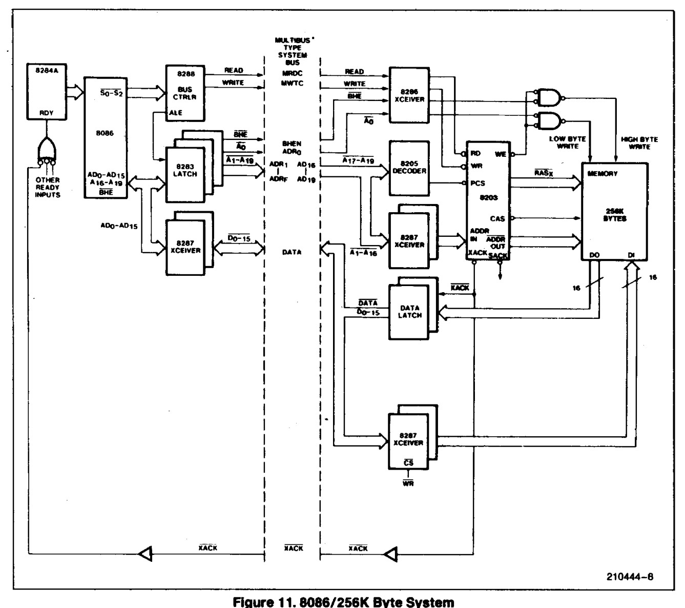
The guys on the SEBHC list and I had a talk about DRAM solid state disk S100 boards, both a Semidisk board (which I actually own) and a compupro board (which I don’t own, but documentation exists for). Both of these boards used the D8203, so there were some working implementations. These were not general purpose memory board, but were semiconductor disks address via io ports. As the schematic for the compupro board existed, I tried to leverage it.
Compupro used a flipflop like my Failure #3, but their engineers kinda inverted the way it worked. The compupro board clocked in a ‘0’ on MEMW or MEMR, and then used /XACK to clear the flipflop. Same basic strategy as my approach, but a different way of achieving it.
This worked on my 8085 CPU, but it didn’t work on my 8080 or Z80 CPU boards. The problem with the 8080 was that the data didn’t arrive until part way through the /WR cycle, so sometimes I’d miss the data and write zeroes. The problem with the Z80 was that it doesn’t implement waits during the write cycle — it samples WAIT before asserting /WR. So the Z80 wouldn’t implement write wait states and would often miss a write entirely.
Failure #5: Delays and the mother of all complicated solutions
At this point I was working entirely on the Z80 board, and I knew that it wouldn’t let me implement a wait state on write, so I figured what I’d do was to delay the following operation if my wait was running late. I latched the state of the address and data buses, and I used a flipflop to track when my operation was in progress. I would hold the /WR and /RD signals to the D8203 until I saw the XACK. I would hold the WAIT signal to the CPU so the CPU couldn’t implement a new memory operation until I was done. Look at this complicated mess I put into the PLD:
/* connect:
     STARTWAIT to 1CLK
     XACK to 1SET
     +5V (or !RESET) to 1CLR
     GND to 1D
     WAITING to 1Q
     -
     STARTDELAY to D2
     DELAY to DEL2
     -
     10pF / 5.1K on LS123
     20MHz crystal on D8203
     3.3k OR 5.1k resistor same result
     brutprim 100 on 2 MHz Z80: 43 seconds, vs 34 seconds on SRAM board
*/

/* Hold MW from the time it first asserts, until XACK occurs. Force a pause between one
   operation and the next.
*/

MW = !RESET & ((CS & BMEMW & !XACK & !MW & !MR & !DELAY) # (MW & BMEMW) # (MW & WAITING));
MR = !RESET & ((CS & BMEMR & !XACK & !MW & !MR & !DELAY) # (MR & BMEMR) # (MR & WAITING));

STARTDELAY = !RESET & XACK;

STARTWAIT = !RESET & (MW # MR);

WAIT = !RESET & (WAITING & (MW # MR));

CS = CSIN # WAITING; /* hold CS while we're waiting */

LOE = !RESET & CSIN & BMEMR;
OLATCH = XACK;
I had to interject a delay between ending one memory operation and starting the next. The D8203 requires some time between commands. So I added a LS123 delay circuit to ensure that there was a brief pause where no memory operations could occur. It was a complicated and finnicky and ill-performing solution.
It worked sometimes. Unpredictably. The computer would be in a good mood and I could reboot it, or even power it off for a very short while, but if I powered it off too long, it would get into a bad mood where I had to fuss with things and then it would start booting again.
Solution 1: Some random eBay board to the rescue!
Around this time, some H8 DRAM boards appeared on eBay. I lost the auction. But by virtue to creating youtube videos and generally pestering people on forums, I eventually made contact with two people who acquired these vintage 8202-based DRAM boards.
With the help of the community, I reverse-engineered this board without ever having one in my physical possession.
Through the help of two users, David and Willis, I managed to reverse engineer a schematic by way of pictures and of having them probe connections which were not obvious from the pictures. The solution is really quite simple and boils down to three things: Waitng until /SACK, delaying /WE, and implementing early write.
We still don’t know which manufacturer design and built these D8202-based DRAM boards. We have two confirmed owners who bought the eBay auctions and were able to get their boards working. But we don’t have documentation or data on the boards themselves. I did at least, from my reverse engineering effort, learn what the dipswitches and jumpers did.
Solution 1A: Waiting until /SACK
My early attempts were on the right track, but were overly complicated. The wait state can simply be reduced to this:
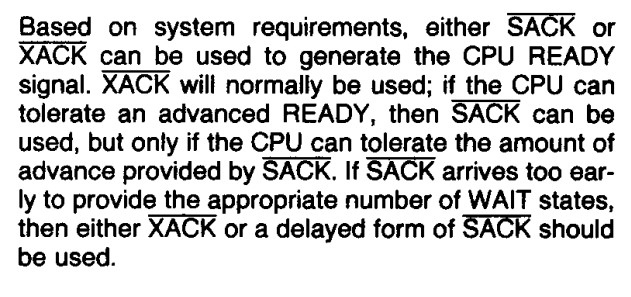
WAIT = (BMEMR # BMEMW) & CSIN & !SACK;You wait if a Read or Write is in progress, and your chip is selected (i.e. this is a memory window you care about), and if /SACK has not been triggered yet. /SACK stands for system acknowledge and is the signal the DRAM controller asserts when it has started working on a memory transaction. It’s similar to /XACK. /SACK is intended to fire when the transaction starts, and /XACK fires when it terminates. Except that sometimes /SACK will occur after /XACK. The datasheet explains this.
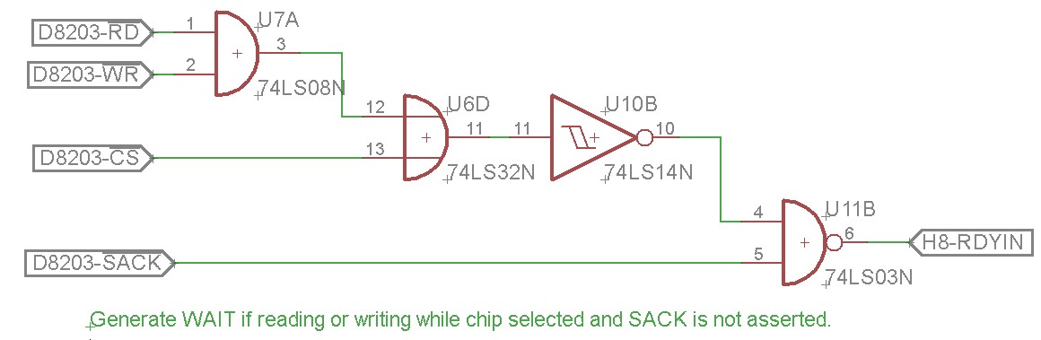
Anyhow, a single simple solution implements the wait state. My 8085 was working!
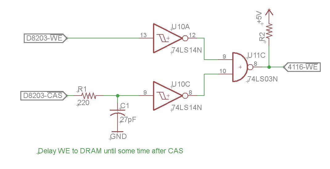
Solution 1B: Delaying /WE
The /SACK based wait strategy managed to get the board working with my 8085 CPU, but not my 8080. The 8080 has the annoying habit of not putting data on the bus until about half way through the /WR cycle. The DRAM ICs actually write data when their /WE signal is asserted, not when it is released. So what happens if we complete a write on the 8080 before the 8080 has put the data bits on the bus. We write a bunch of zeroes.
The eBay board’s solution for this was simple, to delay the /WE signal to the DRAM by about a hundred nanoseconds or so. It does this by a resistor and capacitor on the input to a 74LS14 schmitt trigger inverter. It took some trial and error to get the RC right, but eventually I was able to get the /WE signal to not assert until after the data is on the bus. It’s just a matter of timing.
Solution 1C: Z80 Early Write
I still had one nagging problem. The Z80 /WR cycle is short and it doesn’t pay attention to wait states.
Turns out heathkit has a solution for this, and it’s implemented on the HA-8-6 board:
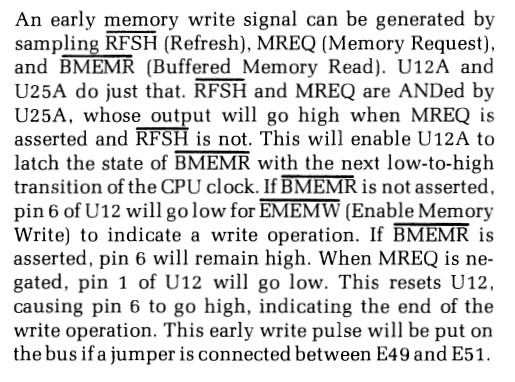
That’s not the easiest thing to read, but it boils down to this — if you’re doing a memory access and it’s not a read, then it must be a write. The HA-8-6 includes a schematic. The schematic has a few errors, but it was easy to sort them out. Below is my revised schematic of the Z80 early write circuit:
I made a small piggyback board that I attached to my SEBHC/Norberto Z80 board that implemented delayed write.
Now let’s look at some timings…
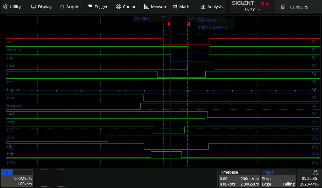
First let’s take a look at the write timing on the 8085,
The 8085 write cycle is fairly simple. BMEMW is the write on the H8 bus. It goes high to start a write transaction. It is followed by a downward /MW, which is simply BMEMW inverted. This will cause the DRAM controller to initiate CAS and then RAS. The WE-delay circuit delays CAS to form CASD, which in turn generates the /WEDRAM signal to the DRAM, which writes the data. Note that on the 8080 BD0 (bus data bit 0) is asserted very close to BMEMW. RDY has the waitstate, and is initiated from the time /MW goes low to the time when /SACK is asserted.
Next let’s take a look at the write timing on an 8080, since it shows a few interesting differences.
On the 8080 first note that the transition of BD0 (bus data bit 0) from high to low happens about 50ns after the BMEMW starts. This is where the delayed write comes into play. The delay from CAS to CASD prevents /WEDRAM from writing the DRAM until after BD0 has settled.
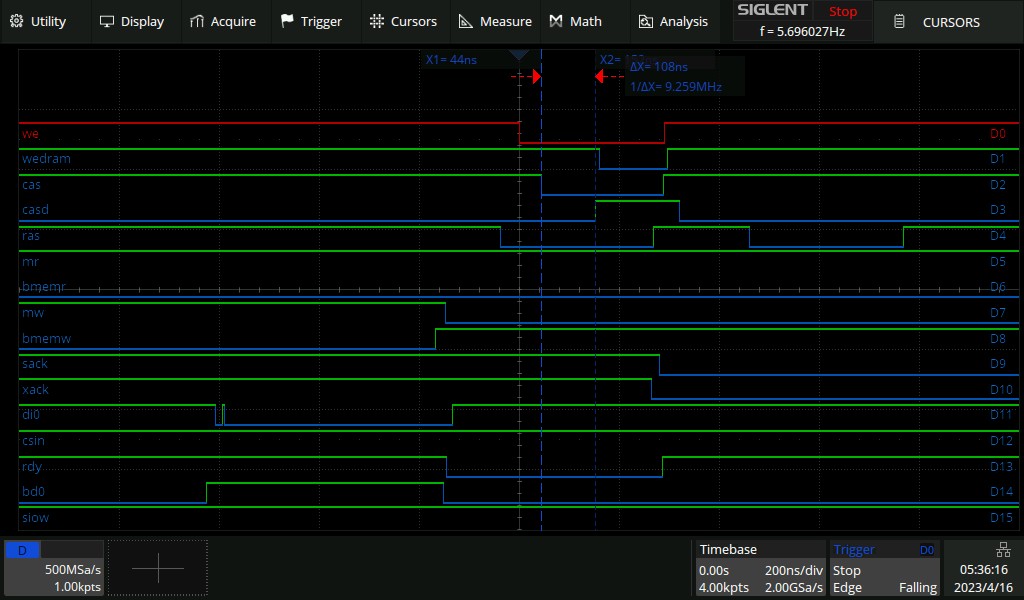
Finally let’s take a look at the early write modification to the Z80 board.
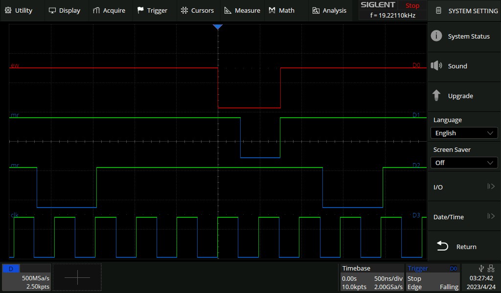
The topmost trace (“EW”) is the early write. The second trace (“MW”) is the BMEMW signal from the bus. We can see that BMEMW normally occurs half-way through the T2 processor state. This missed the opportunity to insert a wait state for writes. The early write (“EW”) signal is generated about half a clock ahead of BMEMW, at the start of T2, and provides opportunity to insert that wait state.
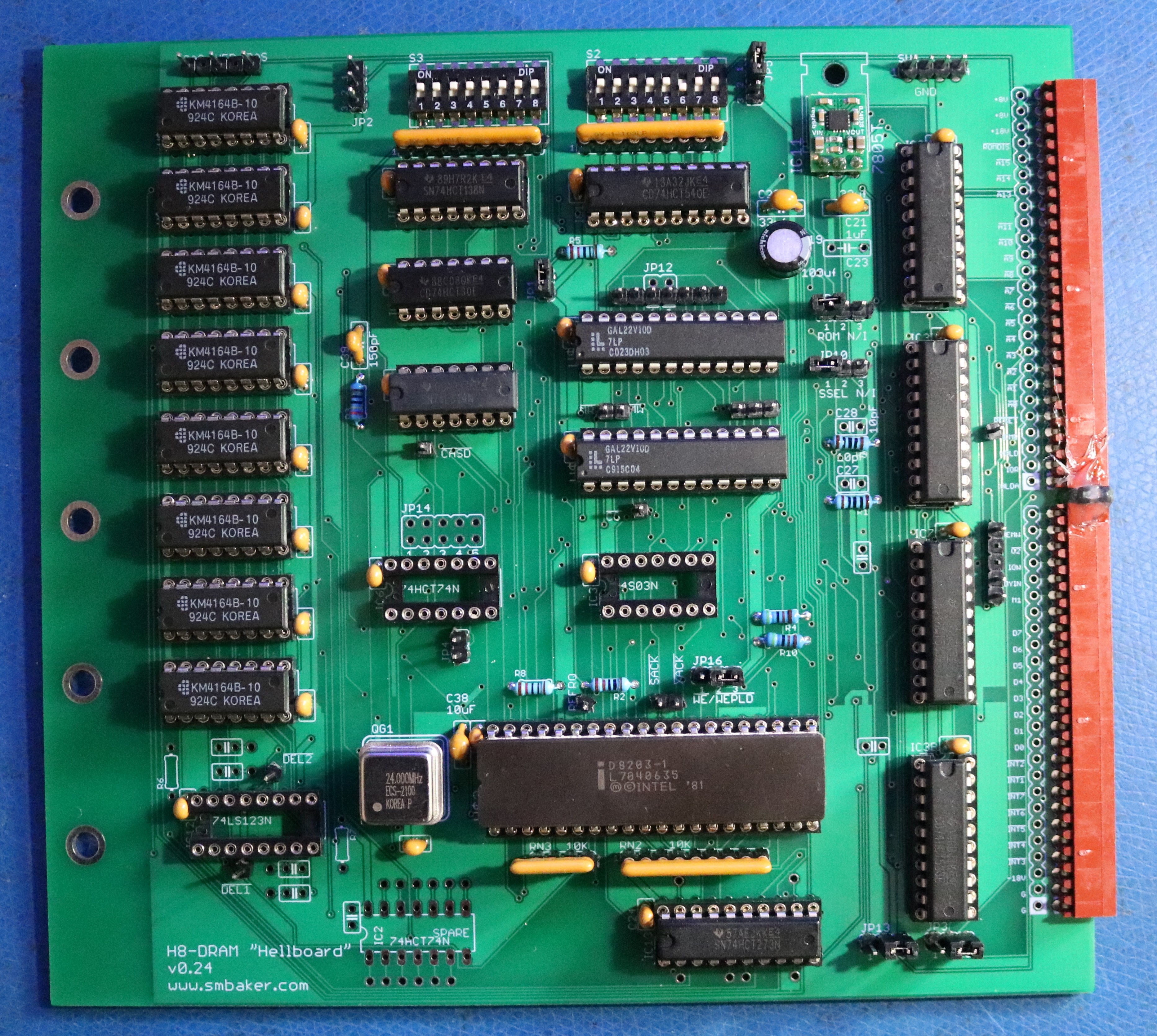
Building the board
If you want to build a board, you need only follow the link at the bottom of this page to the gerbers, which you can order from jlcpcb, and the PLD code which you can burn onto a GAL22V10D with your favorite PLD programmer. The jumper settings on my board are:
| Jumper | Description | Scott’s setting |
| S1 dip switch | selects which 8K memory segments to map | all switches on, to enable all 64K |
| S2 dip switch | org0. see H8-8 documentation. | #6 off, all other switches on. |
| JP1 | board enable | installed |
| JP2 | option OP2 | not populated |
| JP3 | inbound data latch enable (1-2 PLD control, 2-3 always) | 2-3 |
| JP4 | optional flipflop stuff | not populated |
| JP5 | org0 enable. 1-2 to disable, 2-3 to enable | 2-3 when using org0 feature |
| JP9 | org0 ROMDIS polarity. | 1-2 when using org0 feature |
| JP10 | org0 side select polarity | 1-2 when using org0 feature |
| JP13 | address latch enable (1-2 PLD control, 2-3 always) | 2-3 |
| JP16` | delayed write to DRAM. 1-2 no delay, 2-3 delay. | 2-3 |
| SJ0, SJ5 | (back of pcboard) connects 74S03 to MW and MR | do not populate |
| SJ7, SJ8 | (back of pcboard) determines polarity of incoming BMEMR and BMEMW signals. toward-h8-bus-connector = inverted, toward-DRAM = not inverted. | solder each one toward-h8-bus-connector |
| SJ9, SJ10 | BMEMR-to-MR and BMEMW-to-MW | populate each one |
I should have a special mention of the resistor and capacitor used for the WE delay. These are R3 and C39 on the board silkscreen and are marked as 150pF and 220ohm respectively. These need to be set large enough that the 8080 data bus has settled before the DRAM write occurs. I settled on these values experimentally. In my prototype, I upped R3 from 220ohm to 240ohm to provide some additional margin for safety. Your mileage may vary.
Tracking down an HDOS bug
In HDOS3.02 there is an undefined variable at address 0x20D7 (in octal 040-327). If bit2 in this variable is set, then HDOS will wait for hardware handshake before sending output to the serial port. DRAM will generally default to setting 0xFF to this uninitialized variable whereas SRAM may result in other behavior. This was the source of much of my problems throughout the development of the board, with some boot attempts succeeding (“good mood”) and other boot attempts failing (“bad mood”). It took a lot of effort to track down this problem. If using HDOS3, then I recommend setting memory location 040-327 to 000 using the front panel before trying to boot HDOS.
Conclusion and Closing Thoughts
A lot of the problems I experienced were due to the HDOS3.02 uninitialized variable bug that I mentioned above. Were it not for that bug, then it’s possible the second solution that I designed might have actually worked, at least for the 8085. The need to delay the DRAM /WE timing for the 8080 is not something I would have come up with; my plan would have delayed the /WR signal to the D8203.
Working with DRAM is an interesting challenge for someone who is not a formally trained hardware engineer. Most of the vintage computer work we do these days is with static RAM due to the wide availability of large cheap static memories — a single 512K AS6C4008 IC can replace almost this entire board, eight times over! DRAM presents timing challenges.