In this video, I design a CPU board that uses the Intel 8085 Microprocessor, circa 1976.
Purpose / Background
The Heathkit H8 computer originally shipped with an Intel 8080 CPU running at 2 MHz. Popular upgrades included Z80 CPU boards, often running at 4 MHz or even higher. I decided I’d see if I could build a CPU board using the 8085 CPU. I had never used an 8085 CPU before, so this was a new experience:
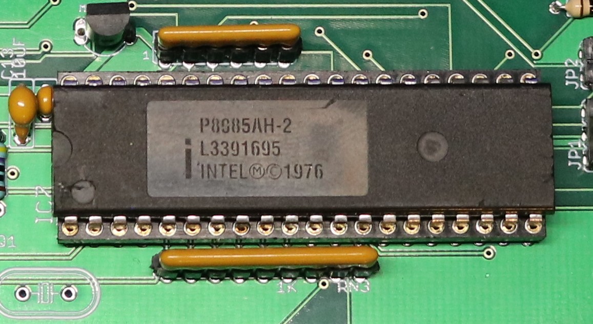
The 8085A-2 features a standard 5 MHz CPU speed. It also has a few additional features, including:
- Full software compatibility with the 8080
- Four additional interrupts
- Dedicated Serial In / Serial Out pins
- Single 5V supply, compared to 8080’s requirements of +5V, -5V, +12V
- Reduced requirement for support ICs. No need for 8224 or 8228
There are a few disadvantages (depending on your perspective):
- The lower 8 address bits are multiplexed onto the same pins as the 8 data bits. This requires an external latch to latch the address bits.
- It lacks some of the 8080’s pins, such as the E1 output.
- There’s no output of the traditional 8080/Z80 “M1” cycle that identifies the first byte (and only the first byte) of an opcode fetch sequence.
Design
The schematics are contained in the github repo, (see bottom of this page), and they’re about 5 pages long, so I’m not going to reproduce them in this post. However, I will talk about a few of the interesting design challenges.
Lack of M1. With an 8080 or Z80 its very easy to decode the M1 signal. The 8085 is not as simple. From the status bits you are able to determine whether or not the CPU is in an “Opcode Fetch” state, but that state is true for all bytes of a multi-byte instruction. The 8080 and Z80 M1 is only asserted for the first byte of a multi-byte instruction. This necessitated some additional logic to create a proper M1 signal. The M1 signal is necessary to determine whether or not interrupts are enabled. I implemented this logic in a custom PLD:
/* for full PLD listing, see github */
/* TMP is an output pin on the PLD, and this allows us to use TMP
 * to store some state even though we're not using TMP as an output
 * pin to drive external device. It can be a little hard to wrap your
 * head around PLD logic that refers back to itself, but if you plot
 * it out on paper, you can see how this works.
 */
M1 = (STATUS:STATUS_OPFETCH) & (!TMP # (M1 & RD));
TMP = (TMP & (STATUS:STATUS_OPFETCH)) # (M1 & RD);
Lack of INTE (interrupt enable) pin. The 8080 includes an interrupt enable output, and the H8 computer uses this pin as part of its single-stepper feature. The single stepper is designed so that it can step through programs, without accidentally stepping into an interrupt handler or critical section, so it disables the single stepper when interrupts are disabled. I borrowed a circuit from Norberto’s Z80 board, which watches the database for EI and DI instructions and computes whether interrupts are enabled. However, this requires the M1 signal that is valid for the first byte (and only the first byte!) of an opcode fetch. This logic is implemented in another PLD, in conjunction with an external flipflop. It might be possible to simplify it down to just a PLD, using self-referring equations as I used for the M1 signal, but doing that gives me a headache.
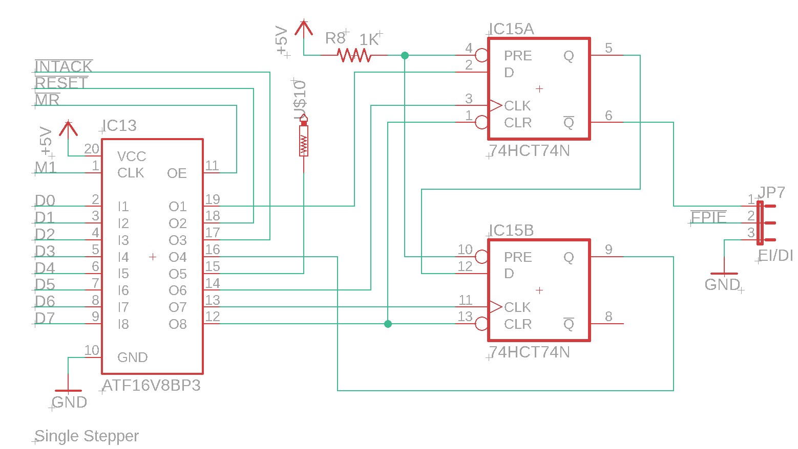
The equations in the PLD to implement this are:
/* for full PLD listing, see github */
FIELD DATA = [D7..D0] ;

$DEFINE EIOP 'b'11111011
$DEFINE DIOP 'b'11110011

TDI = (DATA:DIOP);        /* we need a temporary as !DIOP is expensive to compute */
AD = (DATA:EIOP) # (!TDI & BQ);  /* enable interrupts on an EI, or if we're already enabled and current instr is not DI */

ACLK = !(M1 & MR);        /* Clock is 1->0 when we enter M1, 0->1 when we leave  */
BCLK = !ACLK;
CLR = RESET # INTACK;     /* disable interrupts if reset or intack */
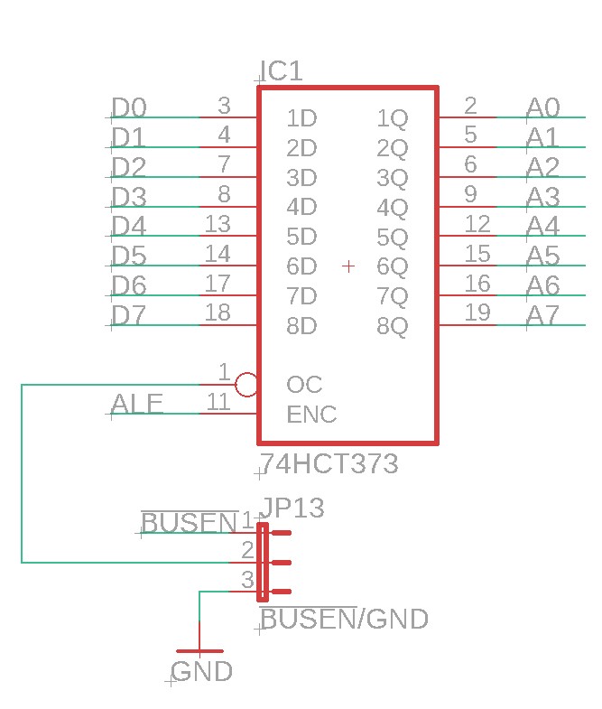
Decoding the address bits. This part is easy. You just use ALE to trigger a latch. The Output Enable of the latch can either be grounded so the address bits are enabled all the time, or it can be enabled only when the CPU is not in HOLD state — in the H8 this doesn’t really matter, as for HOLD we’ll shutoff the transceivers from the board to the BUS, effectively disconnecting the whole board.
Clock generator. It’s relatively easy to drive the H8 clock. You just use a crystal or oscillator that’s double your intended CPU frequency. However, I wanted to have two speeds, a “normal” speed at 2.048 MHz that is compatible with peripherals such as the H17 floppy drive, and a “turbo” speed of approximately 10 MHz that is the maximum operating pseed of the 8085 CPU. This is what I came up with:
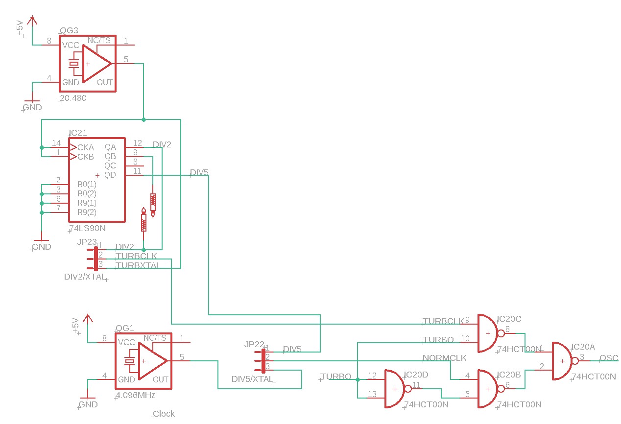
The first option is to use two different oscillators (4.096 MHz for OG1, 10 MHz for OG3). In that configuration, place JP22 and JP23 each in positions 2-3. However, there’s an important drawback with this approach. Simulating frequency switches thousands of times per second, the CPU would occasionally glitch and either halt or misbehave. I believe the reason for this was that the two clocks are not in sync. You could changeover in such a way that a very short clock pulse is generated, glitching the CPU.
For this reason, I can up with an alternative that uses a 74LS90 clock divider. In this case we used a single 20.480 MHz oscillator and divide it by 5 to get 4.096 MHz or by 2 to get 10.240 MHz. As a single oscillator is used, the clocks are perfectly in sync. No chance for any glitches.
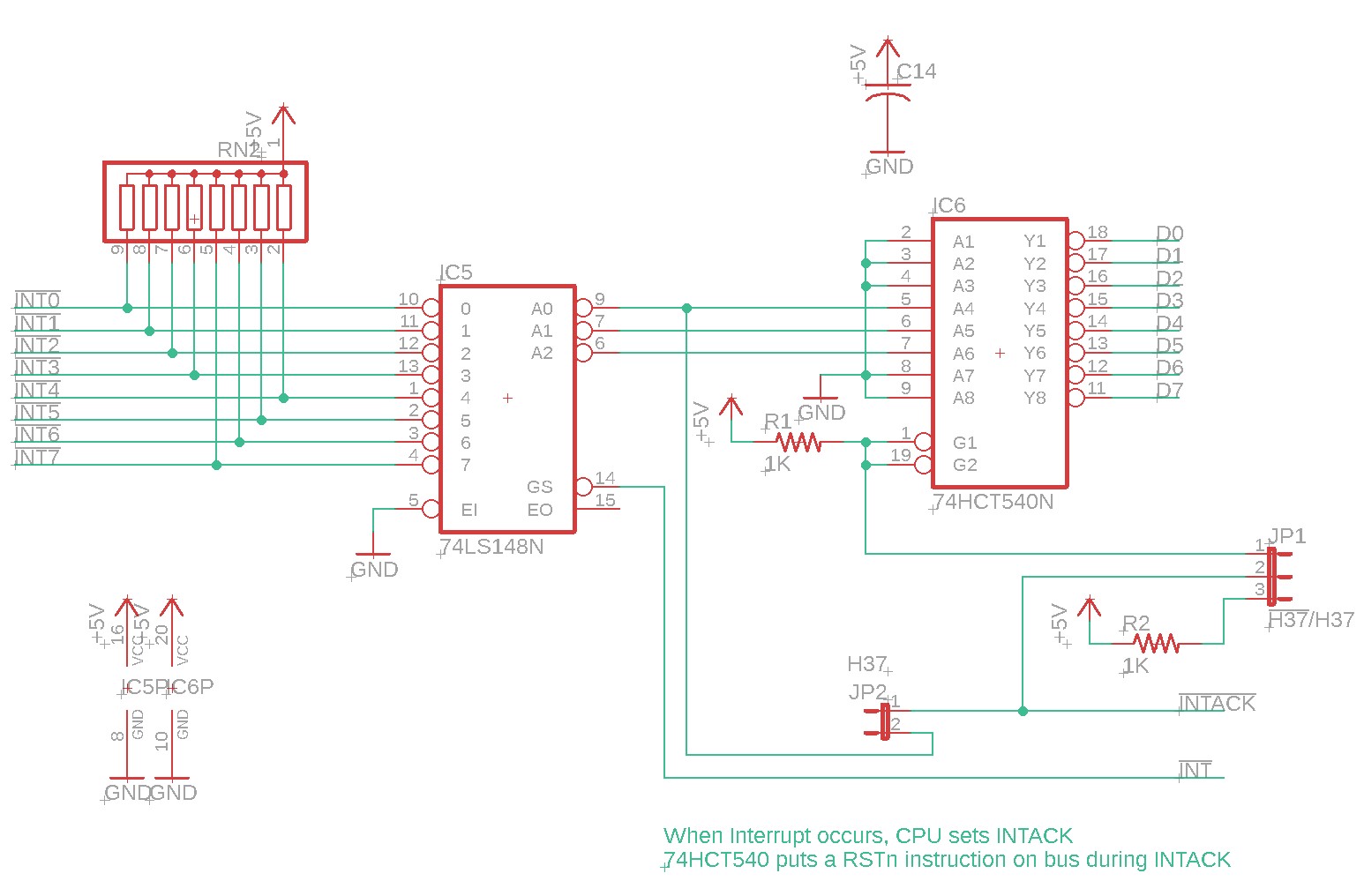
Interrupt Circuit. The standard H8 interrupt circuit uses a 74LS148 encoder to encode one of eight interrupts into three bits, while also generating an INT to the CPU. The CPU responds with INTACK, and the 74HCT540 puts the appropriate RSTn instruction onto the bus to service the appropriate interrupt.
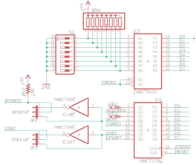
org0 support. The original H8 placed its ROM at address 0. This is, however, incompatible with the CP/M operating system, so Heathkit later came along with something called the “org0” board. Org0 supports includes a read port and a write port. The read port reads an 8-bit dip switch that can be used to configure boot parameters, and the write port’s primary feature is to set the ROM disable and Side-Select bits. ROM Disable will disable the CPU’s ROM, leaving RAM at address 0, supporting CP/M. The Side-Select is used for the H17 disk controller, which initially only supported single-sided disk drives.
Implementation
Below is a picture of the completed H8-8085 board:
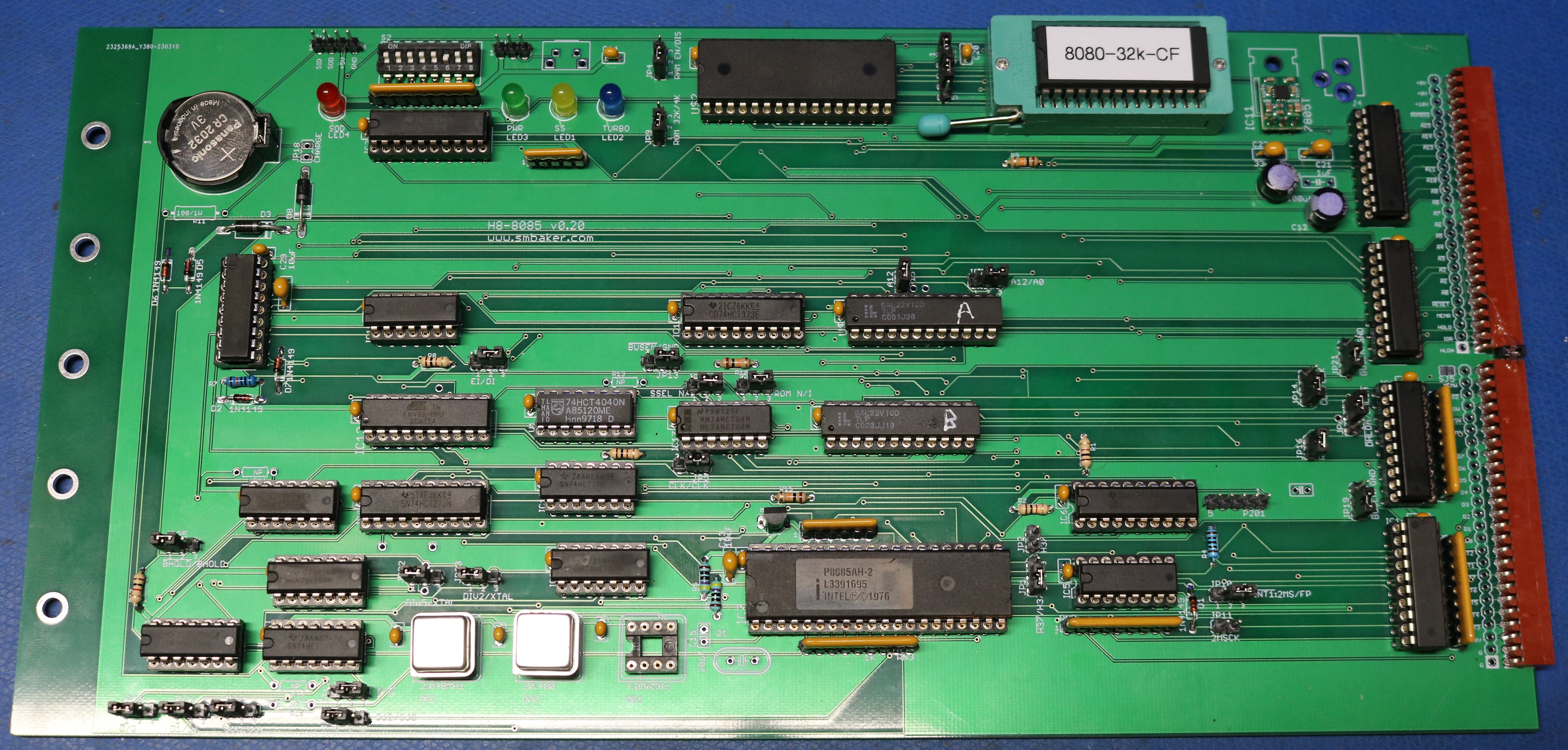
Starting from the top right, we have a ZIF socket for the ROM. You don’t have to use a ZIF socket, but it sure is nice if you reprogram the ROM a lot. To the left of the ROM is an AS6C4008 or AS6C1008 RAM chip. We only use 16 KB of it. Left of the RAM are the org0 swtiches, and finally the batter for the RTC.
Across the bottom, from left-to-right, we have the clock generation circuitry and in the bottom-middle is the 8085 CPU.
Along the right side, by the edge connector, are all the bus transceivers.
Miscellaneous Notes
Jumper settings
See the file JUMPERS.md in the github repo. There are a ton of jumpers on this board, as it was an experimental board that I built many options into.
Instability Issues
I experienced a few problems with board stability, particularly when using the Dual-CF card with this board, and particularly when the physical distance between the CPU board and Dual-CF board was great. I resolved this by replacing my 74HCT640 data bus transceiver with a 74LS640.
I also found, as an alternative to replacing the 74HCT640, that an additional jumper wire from +5V by the regulator (upper right corner) to +5V by the CPU (bottom middle) would reduce the instability problems. I wrote this off to me not using adequate care when laying out the VCC route, which follows a circuitous route around the periphery of the board before it reaches the CPU. Just use the LS640. It’s an easer fix than adding jumper wires to improve VCC routing.
ROM Selection
There are a few ROMs that can be used:
- XCON8 4K ROM (sebhc). If you use the XCON8 4K ROM, then you’ll need to modify the address PLD to switch to 4K addressing instead of 8K. Otherwise, when you boot HDOS3, it will cause you to lose the H17-in-RAM BIOS, and HDOS will get stuck. An alternative is to use an 8K ROM, and put the H17 BIOS in the right place.
- hcfxcon8 ROM (sebhc, modified by me). This is an XCON8 8K image, with the H17 BIOS in the right place, and the Dual-Compactflash driver stuffed into some spare space. It functions with the address PLD set for 8K addressing. This is checked into my github repo.
- 8080-32K ROM (sebhc). This is a 32K 8080 image that includes a serial bootloader and all kinds of nice features. Recommended this is one to go with!
Resources
- My github repository includes the PDF schematics, gerber files, and PLD files in case you’d like to build yourself.
Acknowledgements
Much thanks to Norberto, Glenn, Les, Ken, Joe, Douglas, and countless others on the SEBHC list, who have helped to keep the H8 computer alive and relevant!