In this post, I build an 80186 board for my H8
Introduction
There was some banter on the sebhc mailing list in late 2023 where folks were talking about alternate cpu boards again, including 16-bit boards, boards that used NEC V-20 or V-30 CPUs, etc. At first I thought I would combine both of these and build a 16-bit 8086 board, but then I realized how much complexity that involves — to boot MS-DOS, you typically need a whole plethora of support ICs, including DMA, PIA, Timers, address decoding, etc., in addition to the typical address/data bus multiplexing circuity. If you look at Sergey’s Xi8088 for example, there’s a lot of ICs in that board.
Enter the 80186/80188. I already had experience with the 80188 from building a Retrobrew SBC-188 years ago. The 80186/80188 build many of these additional peripheral ICs right into the CPU package, saving us a lot of board space and complexity. Whereas the SBC-188 used the 80188 and sported an 8-bit external data bus, I wanted to do a 16-bit implementation, so I chose the 80186.
Adapting the SBC-188 design to an 80186 seemed like a conceptually simple task. The SBC-188 already had a BIOS, and that BIOS featured serial port emulation of the video display. Perfect for an H8 Build.
While the board presented here is in the context of being used with the H8 computer and it’s onboard peripherals (H8-4 serial board, front panel, speech synthesizer, etc), the board is also a fully capable single board computer in and of itself with onboard serial I/O and even a 5V barrel jack to power it.
Modifying the SBC-188 for 16-bit
Note: Full schematics will make their way into github… Below contains snippets for the narrative.
Let’s start with the CPU, so we can see all the signals labeled:
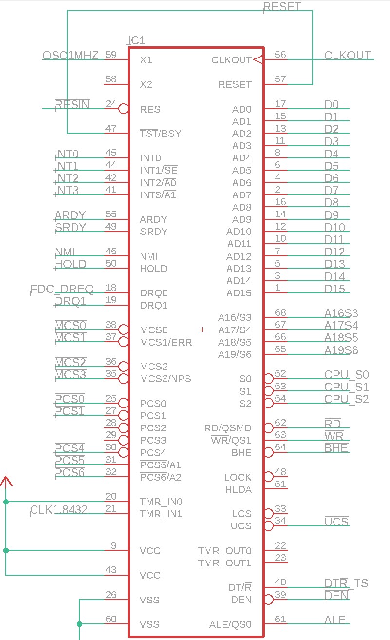
The 80186 and 80188 feature multiplexed address/data buses. Whereas the 80188 has an external 8-bit data bus, the 80186 features an external 16-bit data bus. The situation is analogous to the 8086 and 8088. The basics remain the same — you load your address and control bits from the AD0-AD15 lines when !ALE is strobed. You use AD0-AD15 for data transfer when !DEN is asserted (or in some designs, !DEN is ignored, and you just assume the data bus is in use when you see a !RD or !WR). So this give us our basic address latches:
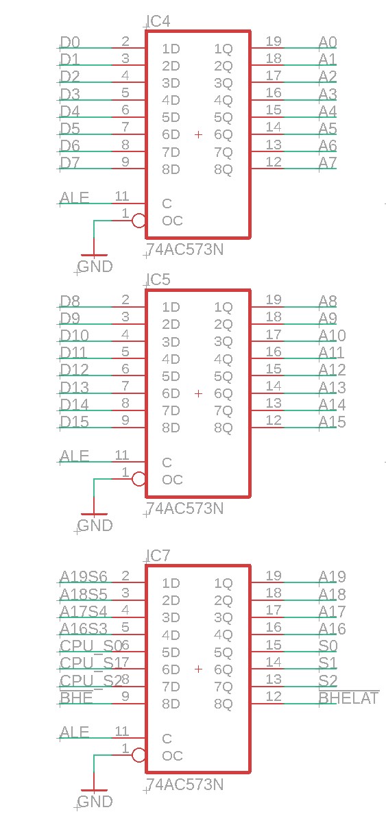
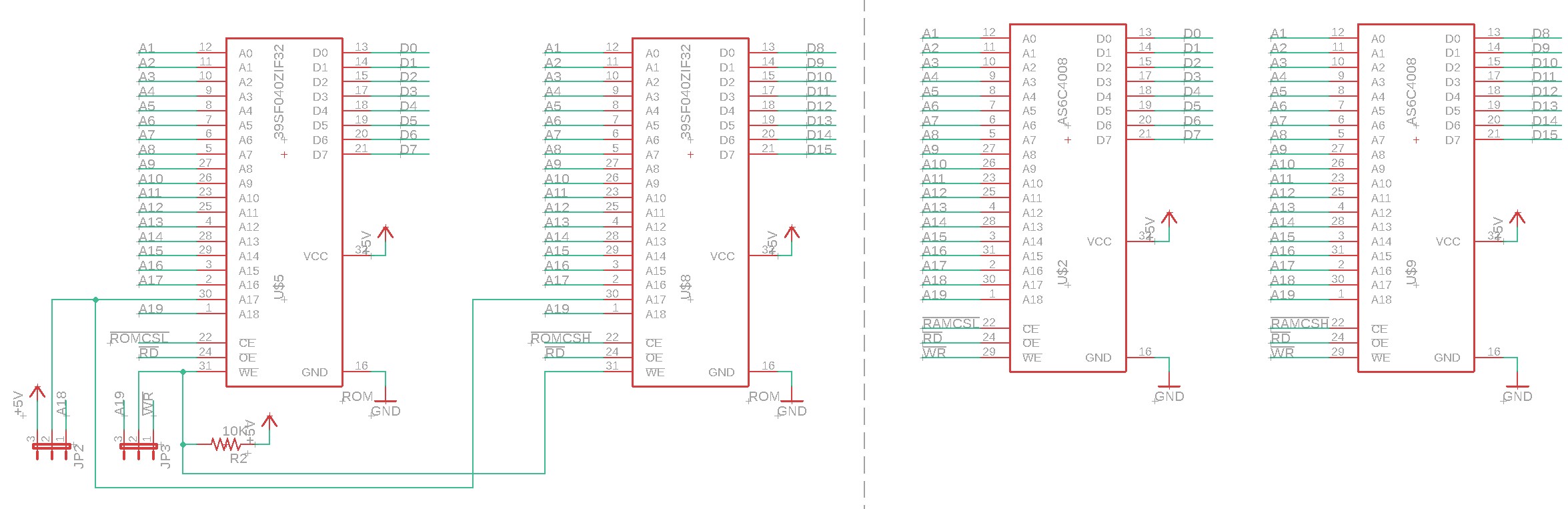
So what do we do about data? Well, the AD0-AD15 pins coming out of the CPU can be plumbed right into out RAM and ROM. We just label them D0-D15 in the schematic. We need 2 RAMs and 2 ROMs, to handle both the upper and lower data bus, so the computer can transfer whole 16-bit words at a time.
There are some signals that tell which part of the data bus we’re using, D0-D7 and/or D8-D15. These are called !BHE and !BLE/A0 respectively. We’ll decode them inside a PLD and use them, together with some memory chip selects, to activate the appropriate ROMs. We don’t want to write a word, if the CPU is only trying to write a BYTE.
This 16-bit fat path is great of ROM and RAM. However, it isn’t really convenient for accessing our I/O peripherals. One easy approach is just to only use the even addresses. The x86 is little-endian, and your even addresses will all go out on D0-D7 and your odd addresses will all go out on D8-D15. However, a lot of software is written to use consecutive addresses, both the evens and the odds. So I used a couple bus transceivers:
Using these two transceivers, we form a new bus, ID0-DI7 the “IO Data Bus”, and we can selectively map either the low bits (D0-D7) or the high bits (D8-D15) to this bus. We’ll only use this for IO operations, not memory, and we’ll hope that nobody ever tries to read or write a 16-bit word in IO space. As long as you only 8-bit transfers with the IN and OUT instructions, then the above will work fine.
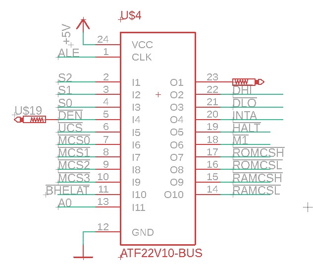
The logic to compute the !DLO and !DHO as well as the !ROMCSL, !ROMCSH, !RAMCSL, !RAMCSH used in the ROM and RAM chips is all contained in the bus PLD.
The full code is available in the github repo, and some of it came from the SBC-188, but the basic idea is this:
IO_OP	=	!ST2 & (!ST1 # !ST0) ;	/* Decode CPU status. INCLUDES -INTA- */

DHI     =       !ALE & DEN & IO_OP & BHE;
DLO     =       !ALE & DEN & IO_OP & BLE;

ROMCSH  =       CSMEM & UCS & BHE;
ROMCSL  =       CSMEM & UCS & BLE;
RAMCSH  =       CSMEM & (!MCS) & (!UCS) & BHE;
RAMCSL  =       CSMEM & (!MCS) & (!UCS) & BLE;
There’s a second PLD that handles the IO addressing
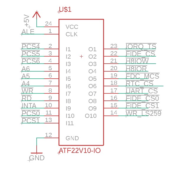
The !PCS0 … !PCS6 signals all correspond to various IO port ranges. The first two, !PCS0 and !PCS1 we’ll map to ports on the H8 bus. !PCS4, !PCS5, and !PCS6 will be mapped to ports on the board. From these PCS signals, together with some address bits, A6..A4, we can generate a variety of chip selects. The PLD code isn’t that interesting so I’ll leave it as an exercise for the reader to check the github repo.
There you have it, that’s really everything that was needed to turn the SBC-188 design into a 16-bit 80186 design. Did I do in the best way possible? Well I can’t say for sure, but this seemed like a decent approach with low complexity.
Connecting the H8 Bus
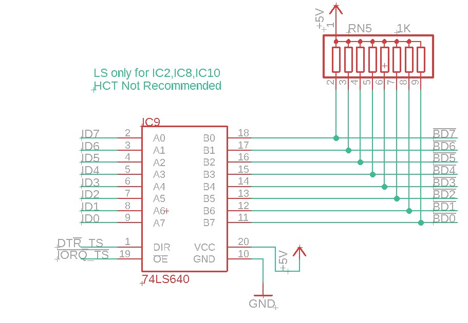
Connecting to the H8 bus is relatively straightforward. We have the IO Data Bus, ID0-ID7, and we have the lower 8 bits of the address bus, A0-A7. There’s no need to implement the upper address bits, A8-A19, as we have no intention of running memory devices on the bus, only IO ports, and the H8 cards typically only use 8-bit addresses for IO ports. The one wrinkle is that the H8 bus uses inverted logic. For example, rather than putting D0 on the bus, it puts !D0 on the bus. For that we’ll use a 74LS640, so we can have bidirectional traffic on the bus:
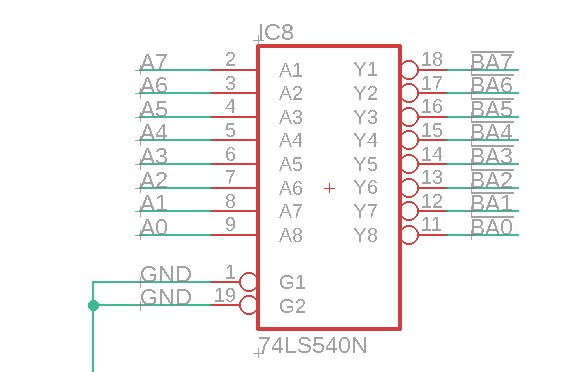
Then we’ll need a similar setup for the address bus, though as the traffic is unidirectional, a 74LS540 will suffice:
There’s a few other considerations in the schematic, such as buffering (and inverting) of the IOW and IOR signals, providing a clock to the H8 bus, etc. I’ll leave you to consult the schematic for more details.
Onboard Peripherals
The board also includes the following:
- 16C450 / 16C550 UART. Having a UART onboard provides the ability to turn this board into a real single board computer, with no other supporting boards. It’s not strictly necessary on the H8, as an H8 owner probably already has a board with 16450 UARTs on it, such as an H8-4. In my video/demo I used the H8’s UART, not the 80186 board’s UART.
- Dallas 1302 RTC. The RTC also provides nonvolatile storage for the BIOS settings. This makes it mandatory, even if you technically don’t care what time of day it is. Version 1 of my h8-80186 board (demoed in the video) uses revision 3 of the SBC-188 as its basis, and plumbs the DS1302 through the UART’s CS, DTR, OUT1, and OUT2 signals. So you need to populate the UART, even if you don’t use the onboard serial. The next version of my H8-80186 board will use a different approach, so the UART will not be necessary to use the RTC.
- WD37C65 Floppy Controller. This allows you to connect an external floppy drive such as a 3.5″ 1.44MB floppy drive. This is optional, but you do need some way to boot DOS, so you either have to use the floppy, the compactflash (or both).
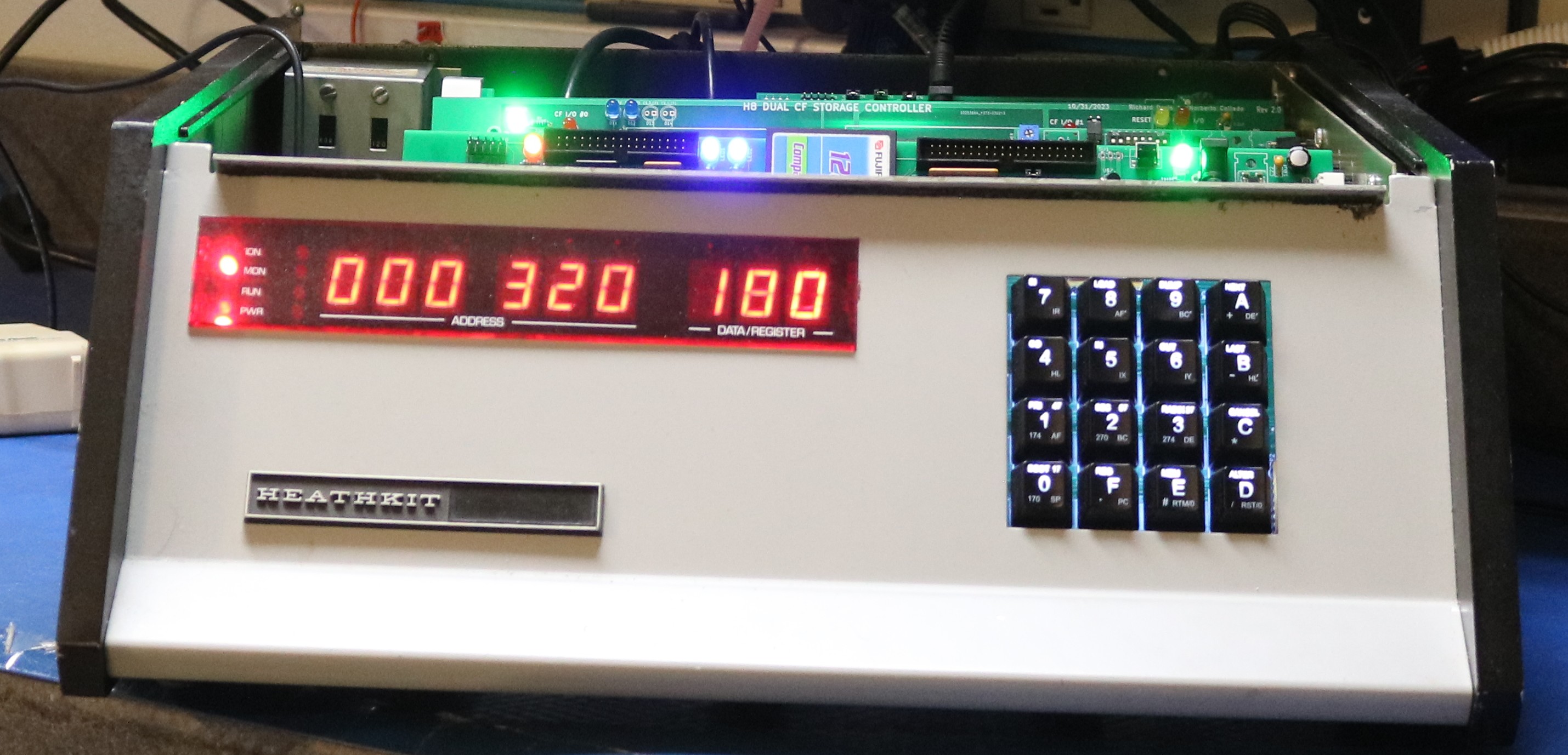
- CompactFlash/IDE8 adapter. The compactflash socket is wired through a simple bidirectional data buffer. It’s operated in 8-bit mode. The CF socket is wired to the adjacent 40-pin header, in case you want to use an external IDE8 device. Note that some CF cards, particularly “very large” ones, may not work right. I had luck with the Fuji 128MB card pictured. I did not have success with a 256MB card I bought on Amazon, nor a 4GB card in my junk box.
All of these peripherals are very similar to what is implemented on the SBC-188. The SBC-188 also included an 8255 parallel port interface, which I did not choose to implement on my board as it led to additional routing complexity to try it fit it in, and such functionality is really not necessary when you already have onboard compactflash.
Bulding the board
A picture of the completed board is below:
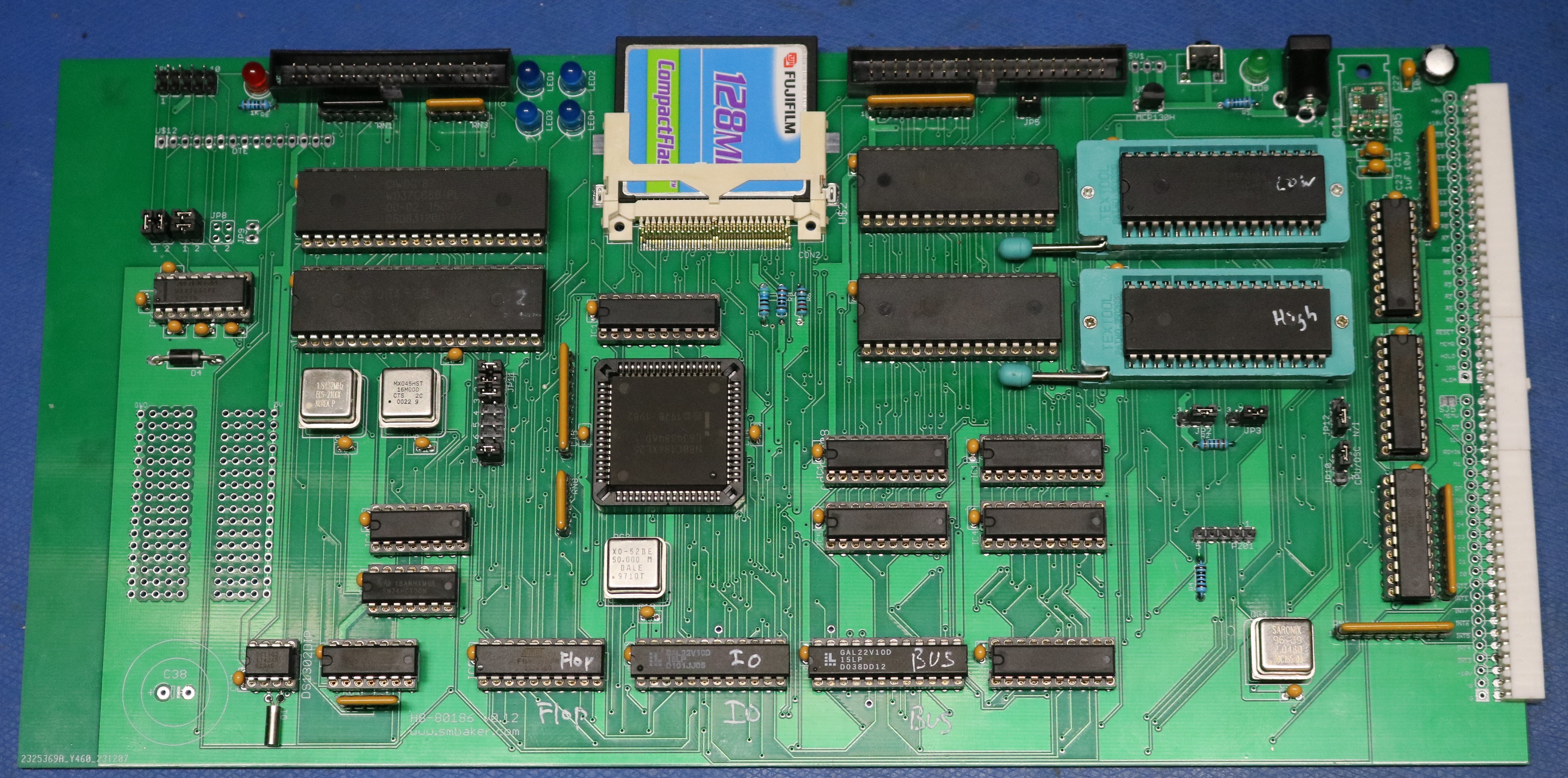
The 80186 is the large chip in the middle. I used an 80C186XL-25, which is good to 25 MHz CPU speed (which uses an oscillator double that == 50 MHz). There’s room for ZIF sockets for the two ROM ICs. There’s both a compactflash socket and an equivalent 8-bit IDE port. The WD37C68 floppy controller is wired to the 34-pin socket. The UART has both a 10-pin socket for a 9-pin DE9 connector as well as the wonky heathkit H8-4 SIP socket.
Front Panel Monitor
The H8’s Panel Monitor (PAM) is an iconic part of the computer. The 8080 PAM won’t work on this 80186 board, but fortunately I’m quite adept at writing front panel monitors, having already written them for the 8008 and the Z8000. In this case, I quickly ported the Z8000 assembly over to x86 assembly and had a front panel monitor working in a few hours.
I first developed the monitor as a separate COM file using NASM. This allowed me to easily copy the monitor over to the computer and run it from the DOS command line. Once I had that working, I went ahead and added it directly to the SBC-188 BIOS.
Software Compatibility
One thing you’ll find out when using either this or the SBC-188 is that software compatibility is hit-or-miss. A lot of software might be expecting exact IBM PC hardware compatibility, which this does not provide. Here are a few notes:
| Software | Notes |
| GW Basic | Mostly works when given the name of a Basic program (.bas file) on the command line. Does not work in interactive mode when launched by itself — pressing return after a keyword does not cause the interactive interpreter to execute it. It’s not known why. |
| Checkit | No output after loading. Locks up computer. |
| Galactic Warzone | Works great! But has a few display issues (status bar issue) |
| Zork1,2,3 | Works great! But make sure to disable the status bar. Zork by default will try to emit ANSI sequences to show its status bar, and the BIOS will strip them out. ANSI.SYS is required, but seems to present its own issues. To disable the status bar, change the third character of setup.inf from ‘Y’ to ‘N’. |
| Any DOS game that uses graphics | Not a chance. |
| Programs compiled with OpenWatcom | You can install OpenWatcom on your Linux (probably Windows too) box, and cross-compile for DOS. I found this worked fine and I was able to compile several programs (lbforth, brutprim, vget, vdir, etc., shown in the video were compiled with OpenWatcom) |
| Programs compiled with Nasm | You can install Nasm on your Linux (probably Windows too) box, and cross-assemble for DOS. I wrote several programs (fpon, fpoff, monitor, etc) and they ran fine. |
Resources
- My Github Repo. It might take me a little while to get everything up here, but I’ll be adding the schematic PDFs, Gerbers, PLD source code, etc.
- The SBC-188 page at Retrobrew. As mentioned above, the SBC-188 was my starting point, and I borrowed everything from the PLD designs to the BIOS source code.