In this post, I build an 8 megabyte memory board… then I install two of them in my Heathkit H8 computer.
Purpose
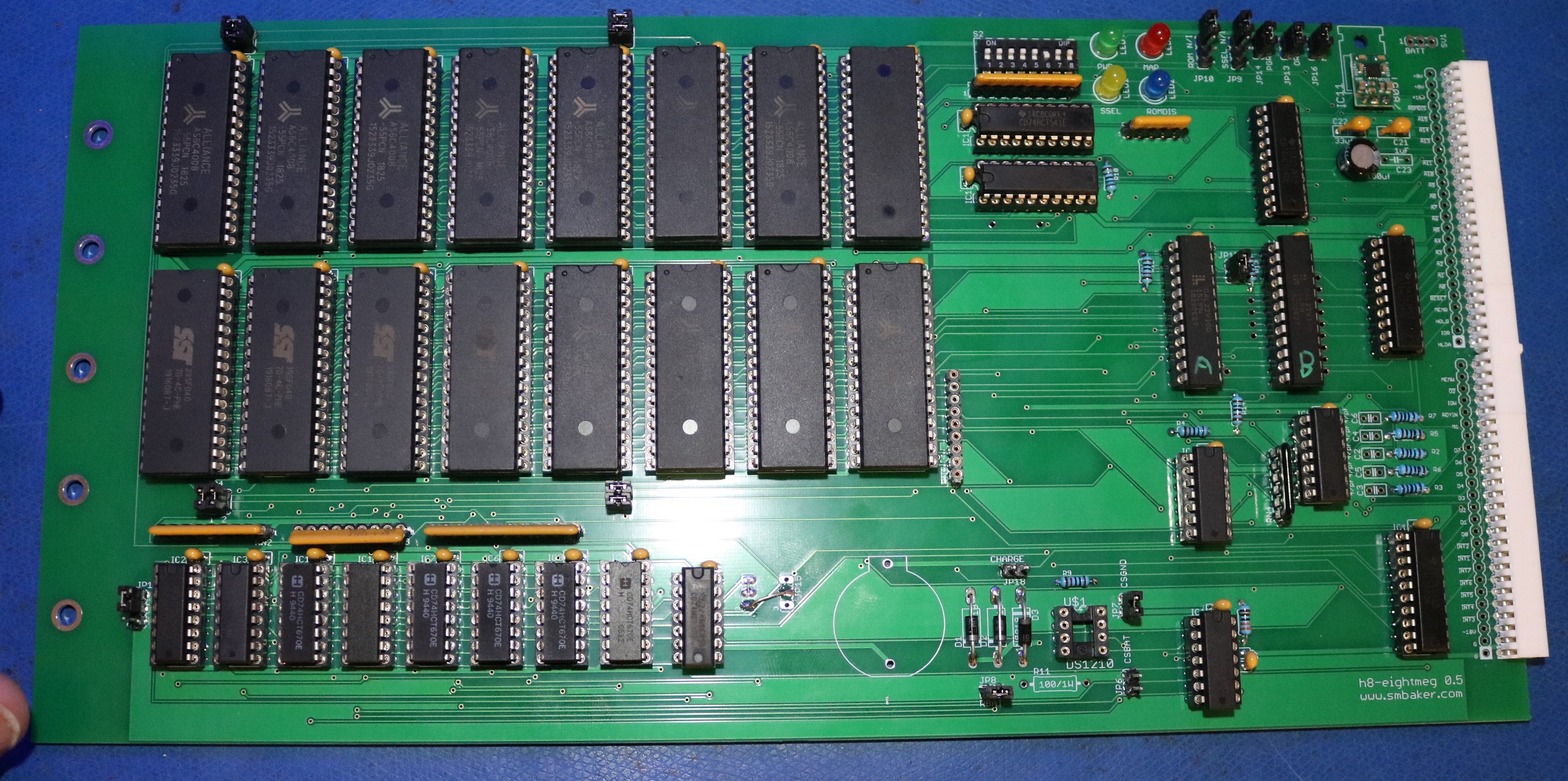
I wanted to see how much RAM I could stuff into an old 8-bit H8. My original plan was to build four boards, and have it be 32 megabytes, but due to a small error in the board design, I ended up with only two boards, for a total of 16 MB. I was also a little short on AS6C4008 SRAM ICs, so I installed about half of it as AS6C4008 and the other half as 39SF040 Flash memory.
So what is this good for? Do you actually need 16 megabytes of RAM in an H8? Probably not… But you can easily use it as a series of ramdisks, each one of them 2MB in size. That gives you room for about eight Ramdisks. SRAM is by nature ephemeral without battery backup, so I designed the board with the intention of using both SRAM and Flash ICs. The flash ICs will be persistent and retain contents at power off. The read performance of SRAM and Flash is identical, but they differ in write behavior — the flash being slower to write and must be written 4KB at a time.
Could you actually use 16 MB for a purpose other than a Ramdisk? I’m sure you could… The memory is pageable in 16KB pages, so you could easily swap data or code in and out of memory.
If you want to build one of these, skip down to the bottom of the page where there’s a link to my github repo with schematics, gerbers, and code.
Background – Memory Mapping
We’re going to use a technique called memory mapping. Here’s a picture that I drew up:
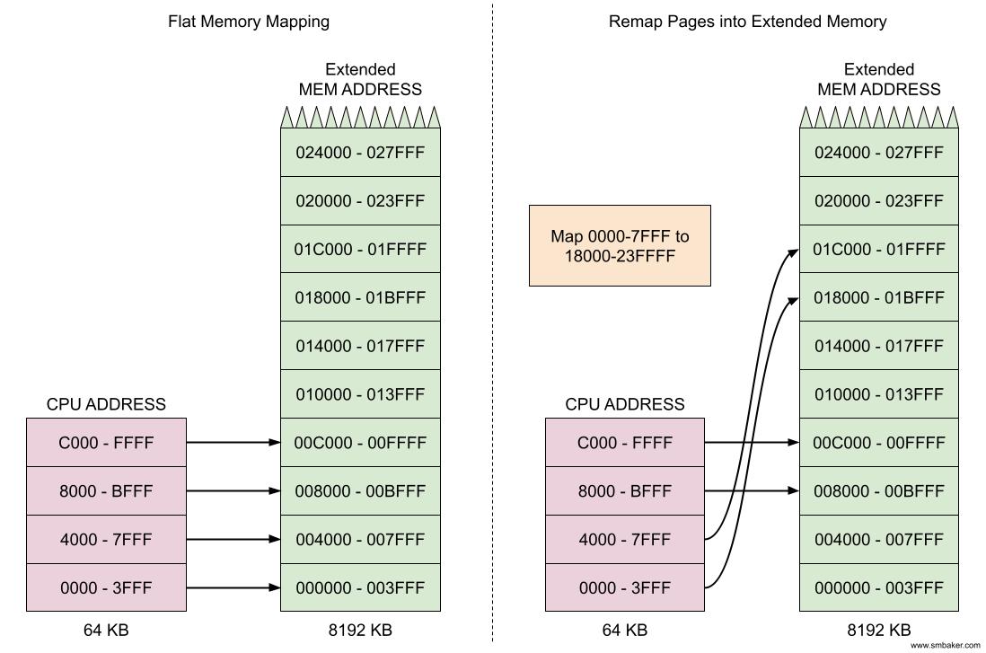
Basically what we do is we use some page registers attached to the A14 and A15 address lines. These page registers can be visualized as arrows that “point to” locations in the extended memory address space. By moving the arrows, we can selectively map 16K chunks of CPU address space to different 16K chunks of memory address space. We have to be a little careful not to map the chunk we’re currently executing from (there are ways to handle that, but they involve some additional complexity). For now, let’s only map the pages we’re not executing — we can easily remap 1, 2, or even 3 pages. The mappings aren’t permanent — under program control we can move the arrows around. This allows us to map really as much address space as we’re willing to create bits within the page registers.
Board Overview
Below is a general overview of the board
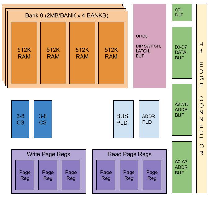
As we can see, it’s divided into several parts
- RAM Banks. Four banks of 2MB each comprised of four 512K RAM chips. This gives us a total of 8MB per board.
- Page registers. 3 each for read and write, allowing for 11 bits worth of paged address space. Separate read and write allows us to map two different pages to the same CPU memory space, so that we can easily copy a page in place.
- 3-8 chip select generators. If we have 16 ICs then we need 16 chip selects. The two 3-8 decoders take 4 bits (MA19-MA22) and translate them into the 16 chip selects.
- BUS and ADDR PLDs. These programmable logic devices implement address decoding, bus logic, etc., and basically replace a handful of 74XX logic with a pair of programmable devices. I used GAL22V10, which are period accurate to the early 1980s.
- Address and data buffers. We need to buffer the signals going to and from the bus, so we use 74HCT540 and 74LS640 buffers. The 540 is unidirectional, for addresses, and the 640 is bidirectional for data.
The IC that we’ll use for mapping is the 74HCT670. Here’s a picture of the page registers:
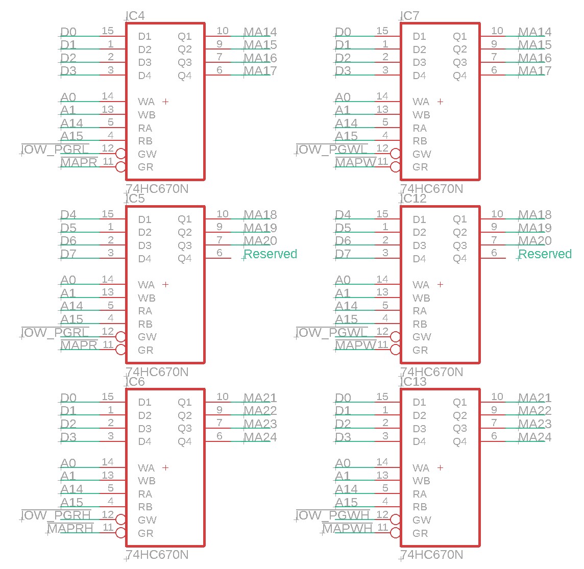
So how does this work? The 670 is what is known as a 4×4 register file. It holds four registers each of 4 bits. The registers are written by the (WA, WB, GW) pins. WA and WB together select which register to write, and GW is the write strobe. They’re read by the (RA, RB, and GR) pins. RA and RB together select which register to read, and GR is the read strobe.
We use the lower address bits (A0, A1) together with some bus decoding from the ADDR PLD to load values into these registers, strobed by IOW. This is done via OUT instructions in 8080 assembly. So we can program these registers under software control, to hold whatever values we want.
Then, when a memory read or write occurs, we read the register using the A14 and A15 address bits. This will provide a whole slew of address lines, MA14-MA24. Those additional address bits afford us 32 Megabytes of virtual addressing space. The A14 and A15 lines are what gives us our 16K chunks of CPU address space.
| A15 | A14 | CPU Address space |
| 0 | 0 | 0000-3FFFF (first 16K) |
| 0 | 1 | 4000-7FFFF (second 16K) |
| 1 | 0 | 8000-BFFF (third 16K) |
| 1 | 1 | C000-FFFF (last 16K) |
The MA14-24 lines will map into a section of the extended memory. For example:
| MA24…MA14 | Address |
| 00000000000 | 000000-003FFF (first 16K of board 0, bank 0, chip 0) |
| 00000000001 | 004000-007FFF (second 16K of board 0, bank 0, chip 0) |
| 00000100000 | 080000-087FFF (first 16K of board 0, bank 0, chip 1) |
| 00010000000 | 200000-203FFF (first 16K of board 0, bank 1, chip 0) |
| 01000000000 | 800000-803FFF (first 16K of board 1, bank 0, chip 0) |
Schematics
Rather than going through the schematics, all four pages of them here in the blog post, I’ll point people to the github repo where the schematics are present in PDF format.
Hardware Implementation
Configuration
TODO: Describe jumper settings…
Software Implementation
In order to make use of the board, I wrote a ramdisk driver for Heathkit HDOS. The driver is located in the very same github repo as the board. I supports up to 8 ramdisks, if two boards are installed in the computer. Each ramdisk is 2 megabytes in size, except the first ramdisk, which has to be shortened by 64K, since the first 64K of RAM must be used as general purpose program memory.
Additionally, the driver can be used with the SEBHC 512K MMU Board, and defaults to this backward compatible configuration, restricting the size of RD0 to 512K less 64K = 448 KB. Use SET RD: NOTINY to remove this restriction for users of the 8MB board, and permit RD0 to use 2MB less 64K = 1984 KB.
The Ramdisk is bootable, using the SEBHC 32KB boot ROM. See the github repo for details. You can boot from any of the ramdisks, RD0 through RD7.
Using Flash instead of RAM
RAM is volatile, and absent battery backup, the contents of RAM will be lost when the computer is powered off.
I support using 39SF040 Flash chips instead of AS6C4008 RAM chip. The flash chips are persistent and will survive power-off. The disadvantage of Flash is that it is much more inconvenient to write. I’ve provided an image copy tool, RDCOPY.ABS to allow RAM to be burned to Flash. For example RDCOPY RD3:=RD1 would copy the contents of the Ramdisk RD1 onto the Flash disk at RD3.
The pinout of 39SF040 and AS6C4008 are different, and a small 2×2 header is present near each bank of 4 ICs. Place jumpers horizontally to use RAM, or vertically to use Flash. Click the board image above and look at the close-up if you are unsure.
Resources
- Github repository. Contains the schematics, gerbers, PLD source and firmware, and ramdisk driver.