In this blog post, I create an 8008 CPU Board for my Heathkit H8
Motivation / Purpose
I’ve made boards for the 8080-based Heathkit H8 with newer CPUs, such as the 8085, but I wanted to try my hand at incorporating something distinctly older. Can it be done? Can switching to an early CPU still yield a functional, useful computer? Yes!
The 8008 is widely regarded as the world’s first 8-bit programmable microprocessor. Ken Shirriff adds some nuance to this in his blog post. I’ll leave it to the computer historians to debate further. The 8008 was certainly before my time, before I ever sat down in front of a computer and started to program.
Challenges
The H8 was designed with the 8080 in mind, and made use of the 8080’s features — the general purpose stack, the robust support for interrupts, the 64KB addressing space, etc. To use the 8008 we’re going to have to make some adjustments:
- Address Space: 16 KB. The 8008 has 14 address bits (A0-13) and therefore only 16 KB of address space. This was generous at a time when many computers only used 4KB or 8KB or memory, or even less. This is one quarter the address space that the H8 has. I have some ways to improve on that; we’ll see further down the page.
- Clock Frequency: The clock frequency of the 8008 is 500 KHz (yes, Kilohertz), with the option for 800 KHz for the 8008-1 variant. This is one quarter the clock frequency of the H8’s 8080 CPU. It means we’re going to be tighter on CPU cycles to tasks such as updating the front panel.
- I/O ports. The 8008 supports 8 input ports and 24 output ports. The H8 in comparison has 256 IO ports, which may be input, output, or bidirectional. H8 devices are typically spread out amongst that port range. A single peripheral device, such as a 16450 UART, can easily consume 8 ports all by itself.
- Limited stack support. The 8008 does support a stack, but the stack is only for holding the program counter. There are no PUSH and POP instructions for pushing and popping other registers to/from the stack.
- Limited interrupt support. The 8008 does support interrupts, but when you have interrupts but lack the ability to save your registers (PUSH/POP), it becomes awfully difficult to implement an interrupt service routine.
Related Work
A couple of other projects helped me greatly along the way:
Schematics
The schematics are about 5 pages long, and you can find them in PDF form in my github repository. I will share some snippets below.
Starting with the basics.
Our 8008 needs a clock:
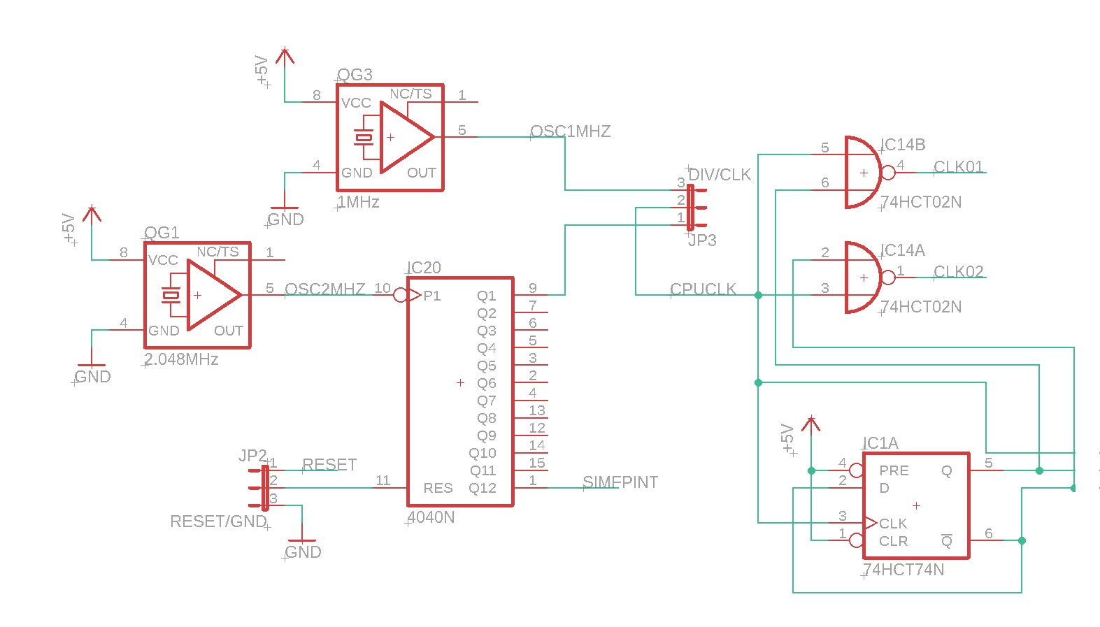
Above we can see the clock. The 8008 requires a two-phase 500 KHz clock, which we can get by taking a 1 MHz clock and subjecting it to a flipflop and a couple of NAND gates. This gets us CLK01 and CLK02. As Len explains in his article, this is slightly out of spec for the 8008, but does seem to work. The H8 also needs a 2 MHz clock for the front panel, so I chose to use a 2 MHz oscillator and divide it in half to get the 1 MHz. I made use of a 4040 divider, because I had in the back of my mind a goal to simulate the H8’s front panel (which also uses a 4040 divider). The 4040 is a bit of overkill for what we need. Next let’s take a look at the reset circuit
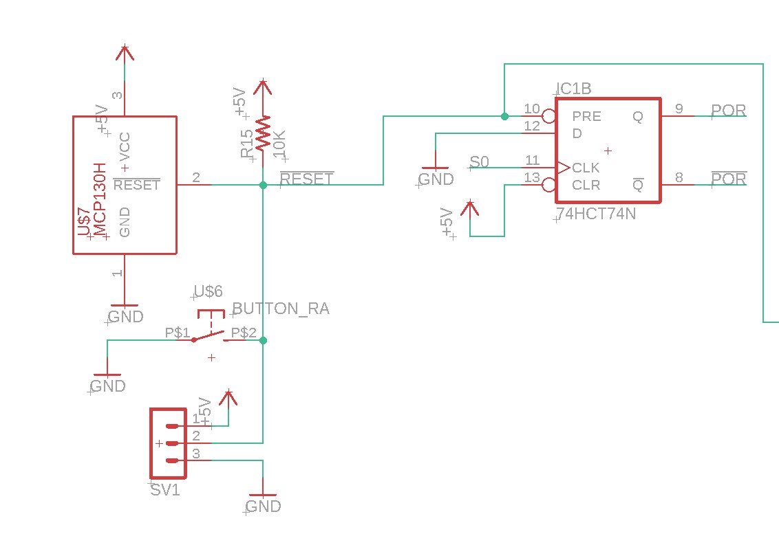
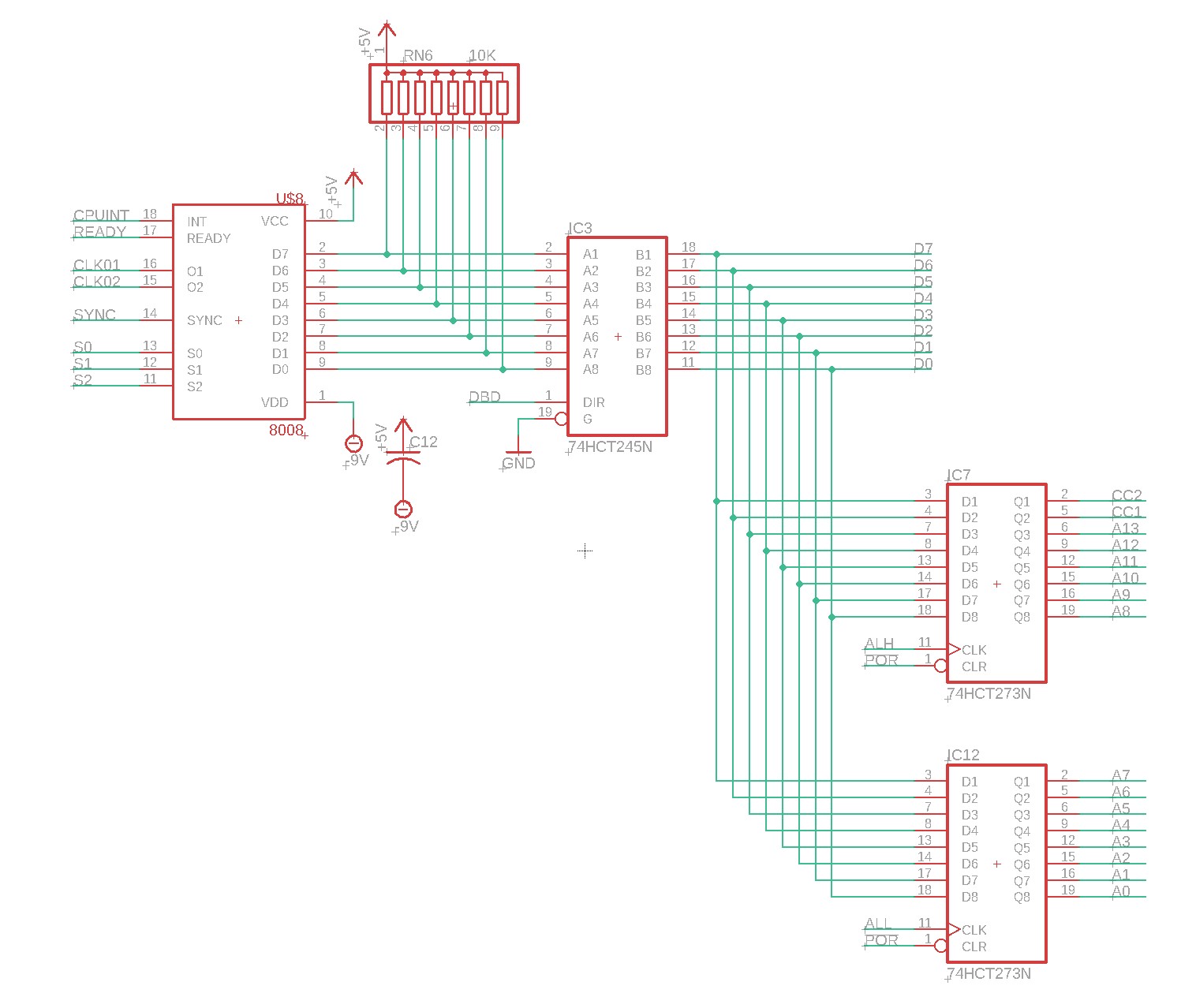
I used the same MCP130 that I’ve been using on my other projects. It’s a supervisory circuit that monitors VCC and holds the reset line low until it’s safe to let the CPU come out of reset. The Flipflop is right out of Jim’s design and is used to assert a power-on-reset (POR) signal until we see some CPU activity on S0. Next we have the bus PLD:
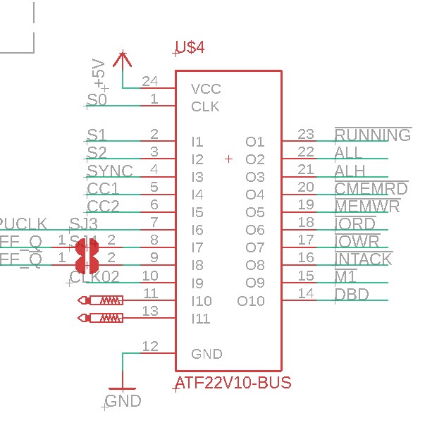
The Job of the bus PLD is to take the CPU state bits (S0, S1, S2, SYNC) and control bits (CC1, CC2) and synthesize the appropriate signals — ALL and ALH for loading addresses, IORD and IOWR for IO operations, MEMRD and MEMRW for memory operations, DBD to signal the data bus direction. We also synthesize a fake M1 signal that the H8 front panel likes. This PLD is more-or-less right out of Jim’s design. The second PLD handles the IO decoding:
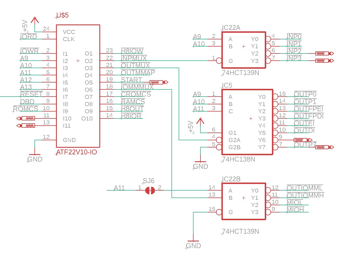
The IO decoder PLD takes the IORD and IOWR signals, and together with the upper address bits (A9-A13) figures out which IO ports you’re trying to use. I ran out of room doing all the IO decoding that I wanted to do, so I made use of some external 2-4 and 3-8 decoders. Basically we decode ports as the following:
- Input port 0 – onboard bitbang serial input, and 4-bit dip switch
- Input port 1 – read state of H8 interrupt signals (see interrupt decoding page)
- Input ports 2-7 – for the H8 bus
- Output port 8 – onboard bitbang serial output, and 4-bits exposed to header pins
- Output port 9 – 8-bit LEDs for debugging
- Output ports 10-13 – these go to the interrupt controller PLD for me to implement interrupts disable/enable logic. Note that ports 12 and 13 are probably not available as I’ll use them in the very next bullet.
- Output ports 12-15 – for memory mapping the 16 KB address space out to 64 KB. To be discussed later
- Output ports 16-23 – for the H8 bus
- Output ports 24-31 – for IO mapping the 8 ports designated above for H8 bus use onto the 256 ports supported by the H8 bus. We’ll talk about that later too.
Next up, let’s look at handling the 8008’s triplexed bus.
The 8008’s bus is triplexed. This means that it serves three purposes: 1) as a data in/out bus, 2) as a lower address bit bus, and 3) as an upper address and control bit bus. The data bus is bidirection (i.e. data goes both in and out) whereas the address buses are unidirectional (addresses only go out). The three state bits in the CPU S0/S1/S2 are used to determine what’s going in and out of these pins on the 8008, and will fire the address latches as appropriate and setup the data direction.
That’s it for the core logic around the CPU. Now let’s talk about how to connect this to the H8.
Interfacing to the H8
I chose to use the H8 bus only for IO purposes, not for memory. There’s plenty of room to just put the memory on the 8008 CPU board itself — the address space is only 16 KB after all. Implementing an IO-only bus is simpler. Let’s start with mapping the IO addresses:
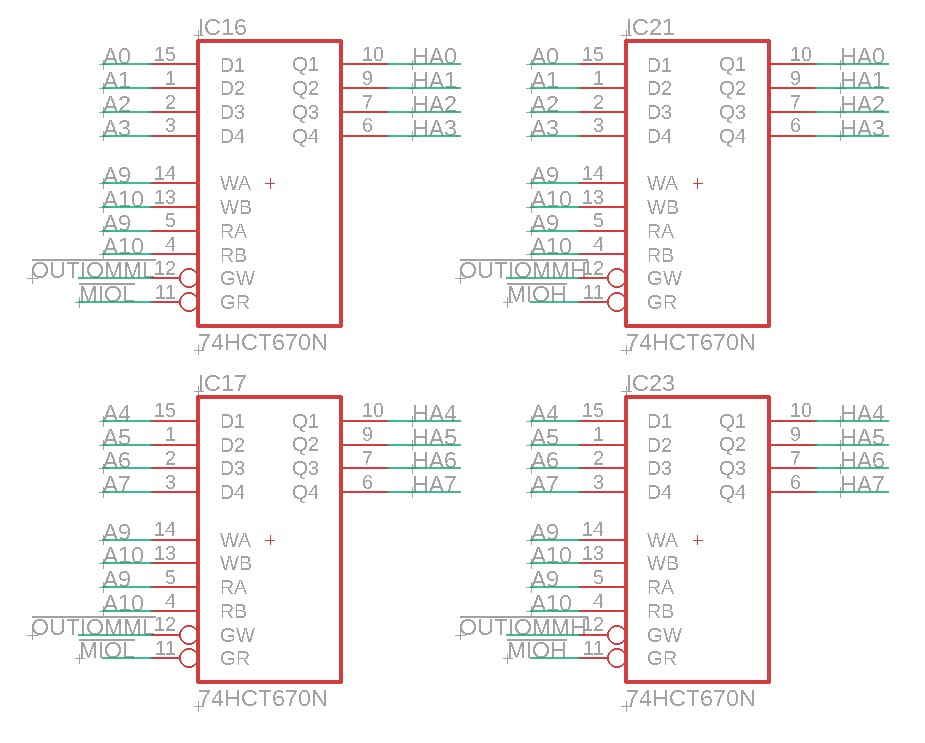
As mentioned above, the 8008 supports only 8 input ports and 24 output ports, many of which we’ve decided to use for other purposes. The H8’s address space includes 256 ports. I used some 74HCT670 4×4 register files to create a general mapping mechanism. You can think of a the 74HCT670 as a sort of miniature dual-ported memory. You can write to it with one set of address bits and read from it with a different set. In this case, we use IO ports 24-31 to write to these 670s. Let’s take IO port 31 for example — if you write an 8-bit value to IO port 31, then that’s the port that will be mapped to the 8008’s input port 7 and output port 23. (this is a little clearer in octal — IO port 037 controls input port 007 and output port 027). This discussion has probably just confused you — if so, go read the code and it will become clear.
Now we have to put those bits onto the H8 bus.
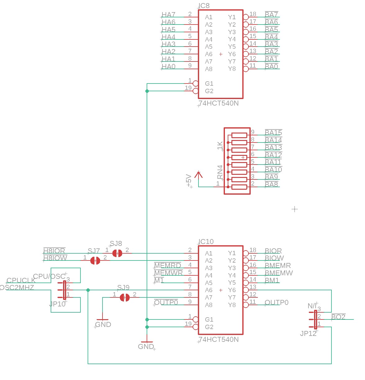
Since I only implemented IO and not memory, I don’t even need A8-A15, so I pulled them up. For A0-A7, I used a simple 74HCT540 buffer to take the outputs of the 74HCT670 register files and put them onto the bus. Recall that the H8’s bus is inverted, and the 540 is an inverting driver. The second 540 buffers a variety of control signals, including IOR and IOW. These are all also inverted. I even buffer and expose MEMR and MEMW even though we don’t use them. Next let’s look at the data buffers:
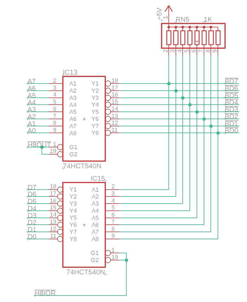
The data lines on the H8 bus are also inverted, and hence we make use of more 74HCT540 inverting drivers. The input direction is simple enough — data comes in from the bus into IC15, and is sent to the CPU on D0..D7. The output direction bears a little more discussion. What’s going on here? It looks like we’re sending the address bits out on the bus?! Why?! Well that’s just how the 8008 does it. When you do an OUT instruction to write to a port, it puts the port address on A9-A13 and it puts the port data on A0-A7. The A0-A7 is what we want to send to the H8 bus.
Memory
Memory is straightforward and makes use of ROM/FLASH/EEPROM/EPROM and RAM. I sort of went with an “all of the above” approach with respect to the ROM footprint, so folks can make use of what parts they have. Any parts that are 32KB or larger ought to suffice. I’ll make sure to document how to set the jumpers for your particular ROM device in the README. To increase the address space from 16KB to 32KB ROM + 32KB RAM, I used a memory mapper:
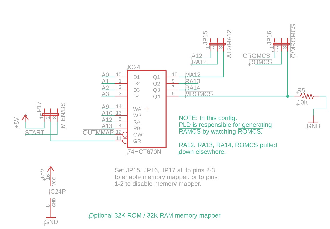
The memory mapper is optional. If you put all the above jumpers in positions 1-2, then you’ll get a fixed 8KB or ROM and 8KB of RAM. If you put them in positions 2-3, then you’ll get the memory mapper. It uses another one of those 4×4 register files. Writing to output ports 12-15 (octal 014-017) will configure 4KB sections of address space. Bit B3 will indicate whether ROM (0) or RAM (1) and bits B0-B2 will determine which 4KB page of the ROM or RAM is mapped.
Implementation
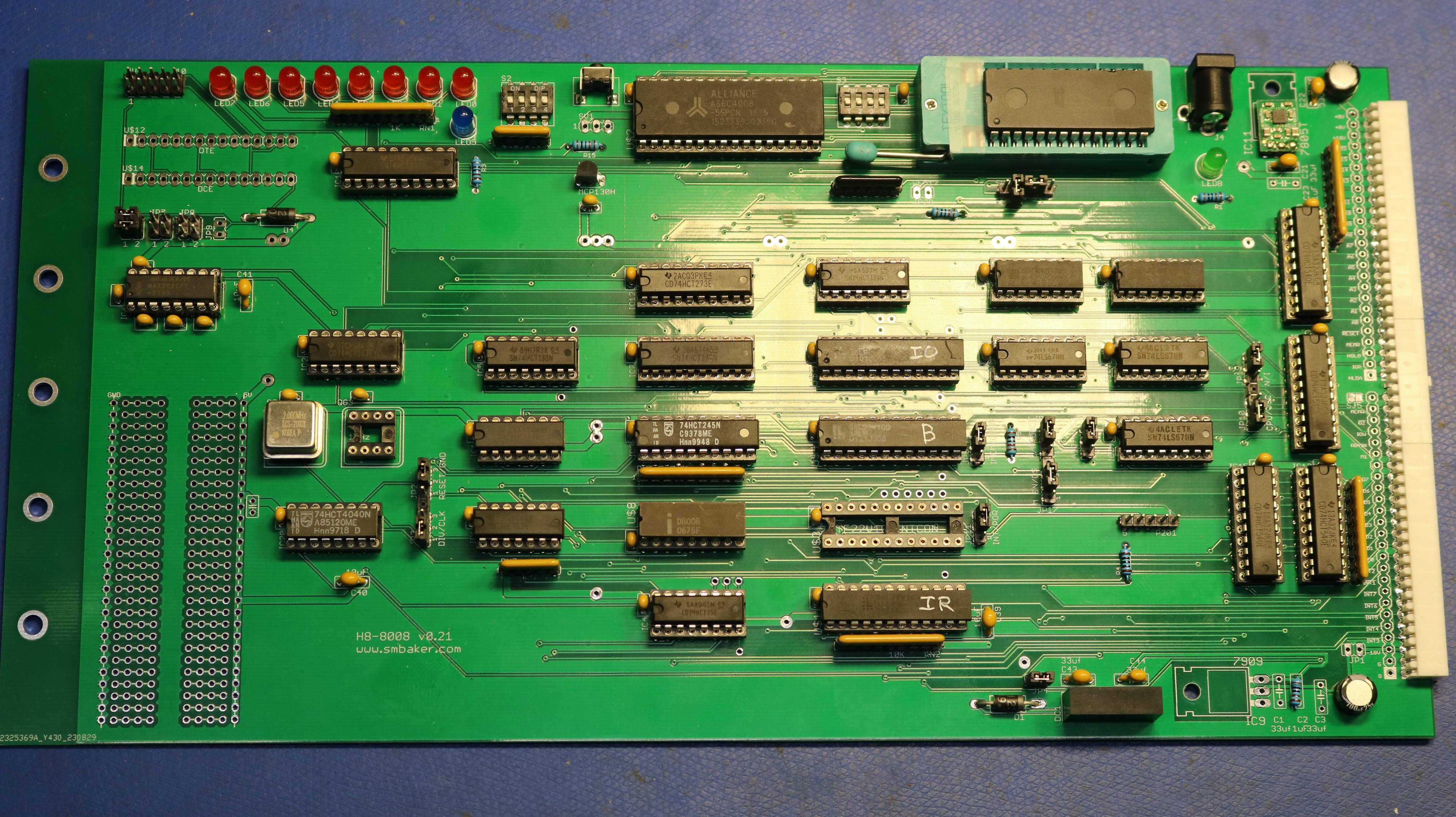
Below is a decent picture of the board:
Using the H8 peripherals
I set out with an objective not to just install a single-board computer into the H8’s case and pretend it’s an integrated computer, but to actually use a couple of the H8’s peripherals. Right now that includes:
- The H8 front panel. The H8 implements this using a pair of IO ports and an interrupt to request display refreshes. It’s not a “set it and forget it” display — you do have to continuously refresh those digits. There’s also a keypad connected to one of these ports as input. Simply making use of the front panel is enough to prove that the H8 bus interface works properly.
- The H8 serial board. The H8-4 serial board contains up to four UARTs. There are numerous aftermarket boards, designed by Norberto, Les, myself, and others that use the same design using 16450/16550 UART ICs. This is much nicer than the bitbang port build into the 8008 CPU board. Given that a 16450 uses a plethora of ports, this is a great example of using the IO mapping register files on the CPU board to expand the 8008’s port space to accommodate additional IO devices.
I’d also like to add some others such as a my H8 speech synthesizer, Norberto’s tape board, or other things like that. Let’s see what all we can do with an 8008!
Software
It doesn’t run HDOS. It doesn’t run CP/M. It doesn’t work with the H8’s panel monitor. It (probably) won’t run any H8 assembly programs.
So what can you do with it once you’ve built it?
- I wrote a panel monitor and grafted it onto Jim Loos’s serial monitor, so we have a basic front panel monitor and a serial monitor. You can examine and alter memory. You can manually input and output from and to the IO ports. You can view a continuously incrementing counter. The panel monitor gives it that iconic H8 experience.
- You can program in BASIC using Scelbi Basic (SCELBAL). As far as basic interpreters go, it’s rather sparse on the feature set, but you can write and execute simple programs.
- You can play Star Trek, Hangman, and a few other games.
- You can write your own assembly programs and burn them to ROM or upload them over serial.
Gerbers, Schematics, PLDs, and Source Code
- My github repo has everything you should need, should you want to reproduce this
Very nice!
Greetings,
Inspired by your memory mapping scheme on the H8 8008 CPU board I decided to attempt something similar on my 8008 SBC. I managed to switch between 8K sections of the 32K EPROM by adding four wires to the existing hardware (and changes to the code, of course). Check it out at: https://github.com/jim11662418/8008-SBC