In this post, I build a compactflash/ide adapter for the Epson QX-10 computer:
Someone did this in 1995…
Some very old posts by Wayne Sung and John D Baker give me some hope this is possible:
A couple of years ago, I was involved in the development of a control chip for a system-independent IDE host adapter. In my case, I built an adapter for my Epson QX-10 to use an IDE hard disk. The interface was fairly simple to build and only minor changes to the BIOS were necessary. The old WD1002-HDO driver routines were 95% correct for controlling the IDE hard disk (first a Conner CP-3022, then a Conner CP-342, and now a Conner CP-3024).
For the record, the only changes made were:
Add 1 to the sector number (IDE starts at sector 1, not 0 [=256]).
Explicitly request a 1-sector transfer.
In the process of making the changes, the old explicit seek code had to be eliminated, but since IDE drives perform implicit seeks on all commands, no functionality was lost.
If you are interested in building an IDE host adapter for your favorite 8-bit machine, you can obtain a system-independent control chip and general schematic from:
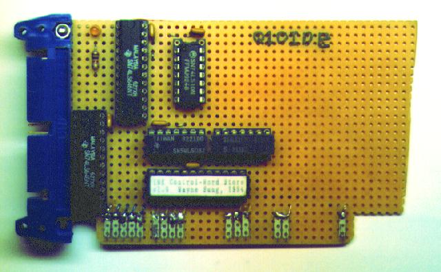
These posts are quite old (circa 1995) if anyone would happen to know Wayne or John, that would be a big help. On the wayback machine, I was even able to find a couple pictures of Wayne hand-made IDE adapter.
Taking a look at the Comrex Comfiler
The Comrex Comfiler was an MFM hard drive for the QX-10. Few of these exist today, but DeltaDon at the VCF Forum was able to send me a couple pictures from the Comfiler’s controller board.
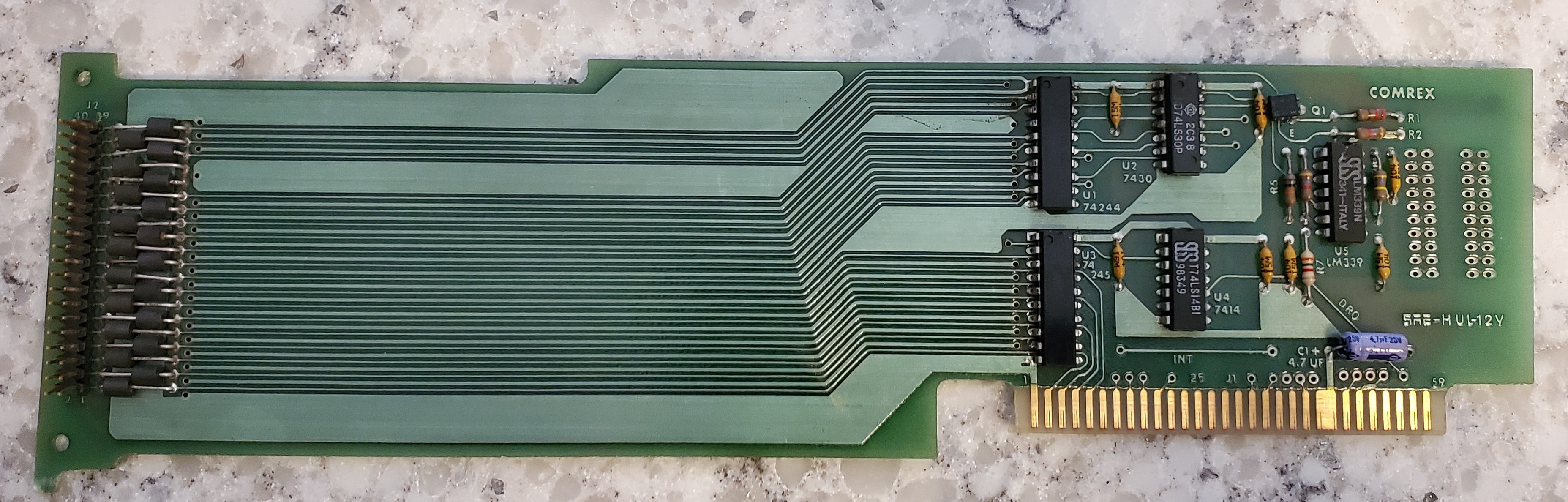
From that I managed to reverse engineer approximately 80% of a schematic.
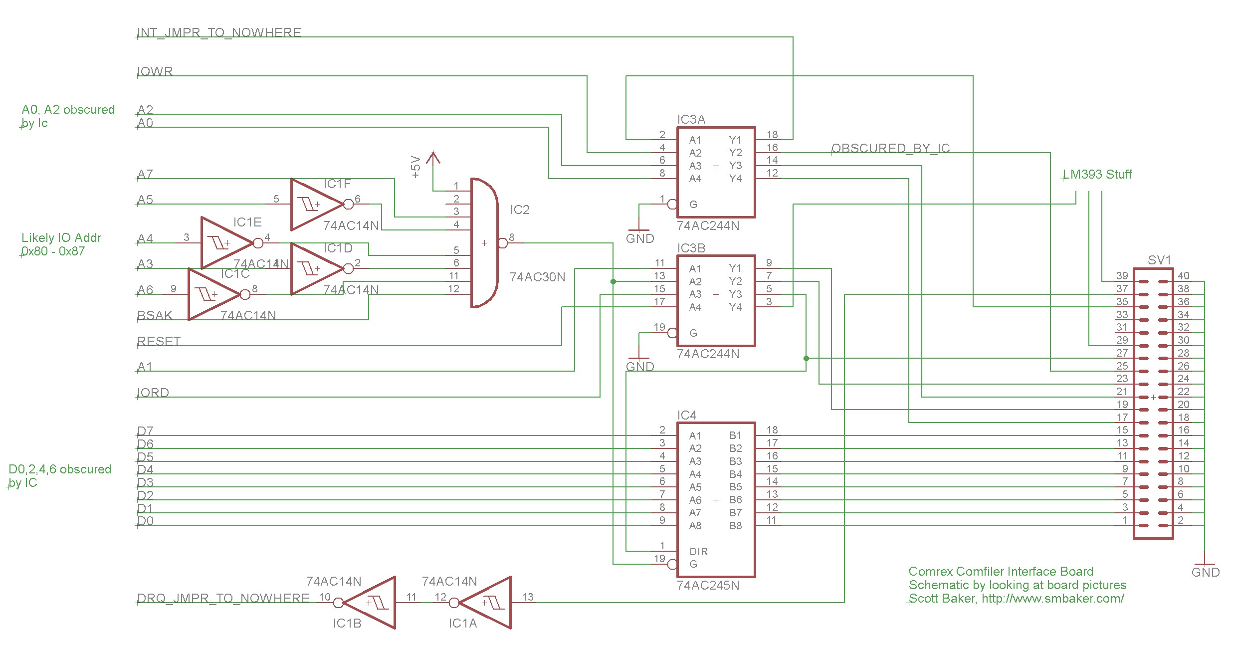
Note: Although the 40-pin connector on the Comrex board might look superficially like an IDE connector, it is not. There would have been either a ribbon cable or a piggyback to another board that would have had the HD controller on it, from what I’ve read, a WD-1002 variant.
The schematic is basically an address decoder, a data buffer, and an address/control buffer. The address decoder appears to decode addresses 0x80 to 0x87, which seems like a reasonable likely location to stick an MFM controller IC. The DRQ and INT lines did not appear to be wired through to the edge connector; maybe comrex build the board with the intention they could be jumpered for advanced use. There’s also an LM339 and some associated resistors and capacitors that I did not bother to map out on the schematic — my working theory is that this formed some sort of reset circuit, perhaps implementing some hysteresis. Several traces I had to take my best guess at as they passed under ICs; if I had an actual Comrex controller then I could do a better job.
Implementing compatible hardware and them patching the driver in the same way that Wayne and John did would be a solution that allowed the existing Epson BIOS to be used.
Another option, the uIDE-8
I found the uIDE-8 from some forum threads by user JonB over at VCF. A wiki page for the uIDE-8 is available at http://www.cpcwiki.eu/index.php/UIDE_Universal_IDE_adapter_cards_for_Z-80_computers. This is a general purpose solution that could be used with most Z80 computers. Compatible hardware would be straightforward to implement on the QX-10 expansion bus.
However, the uIDE-8 driver requires “MOVCPM.COM” to free up some space for the driver.
The lack of MOVCPM and SYSGEN
Investigating the possibility of using Jon’s uIDE drivers, I found that most if not all of the Epson floppy images that I found either do not include MOVCPM and/or do not include SYSGEN. The MOVCPM tool is used to relocate CP/M to free up space where a driver could be installed. It makes use of a relocation bitmap that tells which addresses in the CP/M image need to be fixed up for the relocation. This bitmap is specific to the CP/M that was compiled, and generally you can’t use a MOVCPM from one distribution with a CP/M image from another. It will generate a “Synchronization Error”. You can patch MOVCPM to avoid generating the synchronization error, but even if you do so, the image emitted may not be the image you are looking for.
The next step after a MOVCPM is typically to use a SYSGEN command, which takes the current CP/M image from memory and writes it to the floppy, so that it can be booted next time. The Epson floppies I have omitted SYSGEN as well.
The only Epson floppy that I’ve found that includes MOVCPM and SYSGEN is 2.2 M1.3. This appears to be older than the latest images I’ve found that are 2.2 B2.27.
Understanding the QX-10 BIOS
Poking around CPM2.SYS on the QX-10 floppy, I can see a multitude of INs and OUTs to ports in the 0x80 – 0x87 range. This is enough to prove that the QX-10 CPM has the hard drive code built in. The registers are as follows:
| Addr | Read | Write |
| 0x80 | Data | Data |
| 0x81 | Error | Write Precomp |
| 0x82 | Sector Count | Sector Count |
| 0x83 | Sector Number | Sector Number |
| 0x84 | Cylinder Low | Cylinder Low |
| 0x85 | Cylinder High | Cylinder High |
| 0x86 | Size/Drive/Head | Size/Drive/Head |
| 0x87 | Status | Command |
Disassembling code in CPM2.SYS was a little tricky as I had to find out where it was actually located in memory. The QX-10 is a banked memory computer, and much of the BIOS is stored in Bank 0, while the TPA and program are in Bank 1. Fortunately, there’s a syscall that lets you copy a block between banks. I used this to copy Bank 0: 0x9000 to Bank 1: 0x1000. Here’s my notes on the system call:
; Create a 6-byte block at 0x200 that tells the syscall what to move
S0200
  0 - src bank
  1 - dest bank
  00 90 - src addr 9000
  00 10 - dest addr 1000
  00 10 - count 1000
; Create a short program at 0x100 that executes the syscall
a100
  MVI D,02
  MVI E,00
  MVI C,30
  CALL $F05A
  RST 7
My partial disassembly is as follows:
 99b1: af           xor  a              ; Entry point for Read sector?
 99b2: 32 db 9a     ld   ($9ADB),a
 99b5: ed 5b d0 9a  ld   de,($9AD0)
 99b9: 2a e1 9a     ld   hl,($9AE1)
 99bc: b7           or   a
 99bd: ed 52        sbc  hl,de
 99bf: d2 c6 99     jp   nc,$99C6
 99c2: 3e 01        ld   a,$01
 99c4: 18 31        jr   $99F7
 99c6: cd 5f 9a     call $9A5F          ; Call Seek
 99c9: 3e 20        ld   a,$20
 99cb: d3 87        out  ($87),a        ; HDD Exec CMD - Read Sector
 99cd: 21 00 de     ld   hl,$DE00       ; Destination address to DE00
 99d0: 01 80 00     ld   bc,$0080       ; Read 256 bytes at a time from port 80
 99d3: db 87        in   a,($87)        ; Read Status
 99d5: b7           or   a
 99d6: fa d3 99     jp   m,$99D3        ; Loop while busy bity set
 99d9: ed b2        inir                ; read 256 bytes from port 80 and write to [hl]
 99db: ed b2        inir                ; read 256 bytes from port 80 and write to [hl]
 99dd: 47           ld   b,a
 99de: 3e 30        ld   a,$30
 99e0: d3 86        out  ($86),a        ; select drive 3?
 99e2: 78           ld   a,b
 99e3: e6 01        and  $01
 99e5: c8           ret  z              ; Return
 99e6: 3a cc 9a     ld   a,($9ACC)
 99e9: b7           or   a
 99ea: 78           ld   a,b
 99eb: 28 0a        jr   z,$99F7
 99ed: af           xor  a
 99ee: 32 cc 9a     ld   ($9ACC),a
 99f1: db 81        in   a,($81)
 99f3: e6 10        and  $10
 99f5: 78           ld   a,b
 99f6: c0           ret  nz
 99f7: e6 01        and  $01
 99f9: cd 3a 9a     call $9A3A
 99fc: c3 b1 99     jp   $99B1
 99ff: af           xor  a             ; Entry point for Write sector?
 9a00: 32 db 9a     ld   ($9ADB),a
 9a03: ed 5b d0 9a  ld   de,($9AD0)
 9a07: 2a e1 9a     ld   hl,($9AE1)
 9a0a: b7           or   a
 9a0b: ed 52        sbc  hl,de
 9a0d: d2 14 9a     jp   nc,$9A14
 9a10: 3e 01        ld   a,$01
 9a12: 18 20        jr   $9A34
 9a14: cd 5f 9a     call $9A5F        ; Call Seek
 9a17: 3e 30        ld   a,$30
 9a19: d3 87        out  ($87),a      ; HDD Exec CMD - Write Sector
 9a1b: 21 00 de     ld   hl,$DE00     ; Source address from DE00
 9a1e: 01 80 00     ld   bc,$0080     ; Read 256 bytes at a time from port 80
 9a21: ed b3        otir              ; write 256 bytes to port 80 from [hl]
 9a23: ed b3        otir              ; write 256 bytes to port 80 from [hl]
 9a25: db 87        in   a,($87)      ; Read Status
 9a27: b7           or   a
 9a28: fa 25 9a     jp   m,$9A25      ; Loop while busy bit set
 9a2b: 47           ld   b,a
 9a2c: 3e 30        ld   a,$30
 9a2e: d3 86        out  ($86),a      ; select drive 3?
 9a30: 78           ld   a,b
 9a31: e6 01        and  $01
 9a33: c8           ret  z
 9a34: cd 3a 9a     call $9A3A
 9a37: c3 ff 99     jp   $99FF
 9a3a: 47           ld   b,a
 9a3b: 32 db 9a     ld   ($9ADB),a
 9a3e: 3a 24 27     ld   a,($2724)
 9a41: b7           or   a
 9a42: 78           ld   a,b
 9a43: 28 12        jr   z,$9A57
 9a45: cd 9e 90     call $909E
 9a48: fe 52        cp   $52
 9a4a: c8           ret  z
 9a4b: fe 49        cp   $49
 9a4d: ca 59 9a     jp   z,$9A59
 9a50: fe 43        cp   $43
 9a52: c2 45 9a     jp   nz,$9A45
 9a55: 3e 01        ld   a,$01
 9a57: e1           pop  hl
 9a58: c9           ret
 9a59: e1           pop  hl
 9a5a: af           xor  a
 9a5b: 32 db 9a     ld   ($9ADB),a
 9a5e: c9           ret
 9a5f: 3e a0        ld   a,$A0          ; entry - seek
 9a61: d3 86        out  ($86),a        ; Set SDH to Master, Head0
 9a63: 47           ld   b,a            ; b = A0
 9a64: 2f           cpl                 ; Invert a, a is now 5F
 9a65: d3 84        out  ($84),a        ; Cylinder Number, Low
 9a67: db 86        in   a,($86)        ; Read back the SDH register
 9a69: b8           cp   b              ; Did it change?
 9a6a: c2 c2 9a     jp   nz,$9AC2       ; Yes - Retry
 9a6d: db 87        in   a,($87)        ; Read Status
 9a6f: e6 c0        and  $C0            ; Mask Busy and ready bits
 9a71: fe 40        cp   $40            ; Is drive ready and not busy?
 9a73: c2 c2 9a     jp   nz,$9AC2       ; retry?
 9a76: 2a d0 9a     ld   hl,($9AD0)
 9a79: ed 5b df 9a  ld   de,($9ADF)
 9a7d: 19           add  hl,de
 9a7e: 3a cf 9a     ld   a,($9ACF)      ; Physical drive number and logical drive number
 9a81: 1f           rra
 9a82: d2 8a 9a     jp   nc,$9A8A       ; If logical drive 0, then jump around
 9a85: ed 5b e1 9a  ld   de,($9AE1)     ; de = $0264
 9a89: 19           add  hl,de          ; If logical drive 1, then increase cylinder by $0264
 9a8a: 7d           ld   a,l
 9a8b: e6 03        and  $03            ; Only four heads maximum?
 9a8d: 47           ld   b,a            ; b now has the head
 9a8e: 3a cf 9a     ld   a,($9ACF)      ; Physical drive number and logical drive number
 9a91: 0f           rrca                ; Rotate the logical drive number off the end
 9a92: 87           add  a,a
 9a93: 87           add  a,a
 9a94: 87           add  a,a            ; Shift drive number left 3 times
 9a95: f6 a0        or   $A0
 9a97: b0           or   b
 9a98: d3 86        out  ($86),a        ; Secsize/Drive/Head select
 9a9a: 3a d2 9a     ld   a,($9AD2)
 9a9d: d3 83        out  ($83),a        ; Sector number
 9a9f: 7d           ld   a,l
 9aa0: 1f           rra
 9aa1: 1f           rra                 ; Shift out the head
 9aa2: e6 3f        and  $3F            ; Mask the lower 6 bits
 9aa4: 47           ld   b,a            ; b = bits 0-5 of cylinder
 9aa5: 7c           ld   a,h
 9aa6: 0f           rrca
 9aa7: 0f           rrca
 9aa8: 4f           ld   c,a
 9aa9: e6 c0        and  $C0            ; a = bits 6-7 of cylinder
 9aab: b0           or   b              ; a = bits 0-7 of cylinder
 9aac: d3 84        out  ($84),a        ; Cylinder Number, Low
 9aae: 79           ld   a,c
 9aaf: e6 03        and  $03            ; a = bits 8-9 of cylinder
 9ab1: d3 85        out  ($85),a        ; Cylinder Number, High 2 bits
 9ab3: 3a cd 9a     ld   a,($9ACD)
 9ab6: b7           or   a
 9ab7: 3e 70        ld   a,$70
 9ab9: d3 87        out  ($87),a        ; HDD Exec CMD - SEEK
 9abb: db 87        in   a,($87)
 9abd: a7           and  a
 9abe: fa bb 9a     jp   m,$9ABB        ; Loop while busy bit set
 9ac1: c9           ret
 9ac2: 3e 05        ld   a,$05          ; probable retry point
 9ac4: 32 cd 9a     ld   ($9ACD),a
 9ac7: cd 9e 90     call $909E
 9aca: 18 93        jr   $9A5F          ; JMP Seek
 9acc: 00           nop
 9acd: 00           nop
 9ace: 00           nop
 9acf: 00           nop                 ; logical drive in bit0, physical drive in bit1
 9ad0: 00           nop                 ; 16 bits, head in lower 2 bits, followed by 10 bit cyl
 9ad1: 00           nop
 9ad2: 00           nop                 ; Sector number
 9ad3: 00           nop
 9ad4: 00           nop
 9ad5: 00           nop
 9ad6: 00           nop
 9ad7: 00           nop
 9ad8: 00           nop
 9ad9: 00           nop
 9ada: 00           nop
 9adb: 00           nop
 9adc: 00           nop
 9add: 00           nop
 9ade: 00           nop
 9adf: 00           nop                 ; 16 bits, head in lower 2 bits, followed by 10 bit cyl
 9ae0: 00           nop
 9ae1: 64           ld   h,h            ; (data) 16 bits, midpoint between partitions 0 and 1
 9ae2: 02           ld   (bc),a         ; (data, part of above)
 9ae3: c9           ret
The code is a bit long, and I’m not sure I have the disassembly completely right, but we can see what Wayne Sung was talking about in his comment. The subroutine at 9A5F performs the seek. If we modify this to increase the cylinder number by 1, then we ought to be most of the way there. Or so I thought. Turns out it took me a little more work, but here is my revised seek function:
       .ORG 9a5fh

       ld   a,$A0          ; SUBROUTINE - seek
       out  ($86),a        ; Set SDH to Master, Head0
       ld   b,a            ; b = $A0

       ld    a, $01
       out   ($81), a      ; 8-bit mode

       in   a,($86)        ; Read back the SDH register
       cp   b              ; Did it change?
       jp   nz,$9AC2       ; Yes - Retry

       ld    A, $EF        ; Set feature command
       out   ($87), a      ; execute

BUSWT:
       in   a,($87)        ; Read Status
       bit  7, A
       jr   nz,BUSWT       ; Busy?
       bit  6, A
       jp   z, $9AC2       ; Not ready? Retry

       ld   hl,($9AD0)
       ld   de,($9ADF)
       add  hl,de
       ld   a,($9ACF)      ; Physical drive number and logical drive number
       rra
       jp   nc,LD0         ; If logical drive 0, then jump around
       ld   de,($9AE1)     ; (de) contains $0264
       add  hl,de          ; If logical drive 1, then increase cylinder by $0264
LD0:   ld   a,l
       and  $03            ; Only four heads maximum?
       ld   b,a            ; b now has the head
       ld   a,($9ACF)      ; Physical drive number and logical drive number
       rrca                ; Rotate the logical drive number off the end
       add  a,a
       add  a,a
       add  a,a            ; Shift drive number left 3 times
       or   $A0
       or   b
       out  ($86),a        ; Secsize/Drive/Head select
       ld   a,($9AD2)

       inc   a
       out   ($83),a        ; Sector number plus 1
       ld    a,l
       rra
       rra
       and   $3F
       ld    b, a
       ld    a, h
       rrca
       rrca
       ld    c, a
       and   $C0
       or    b
       out   ($84), a
       ld    a,c
       and   $03
       out   ($85), a

       ld    a, $01
       out   ($82), a      ; Sector count to 1

       ld    a, $50       ; Return from seek would have been RDY+SKC. May not matter.

       ret                ; return at address 9ac1
I had to do a few extra things than I expected. First, I had to put the IDE device into 8-bit mode. Otherwise it’ll operate in 16-bit mode, and we’ll miss half of each transfer. Second, I had to write a “1” to port 82. This sets the sector count. The WD1002 had some bits in the CMD that would toggle between single-sector and multi-sector operations. IDE does not — it solely uses port 82.
There was still one more fix that was needed:
       .ORG 9a14h

       call $9A5F
       ld   a,$30
       out  ($87),a        ; Write Sector
       ld   hl,$DE00       ; HL to address buffer at DE00
       ld   bc,$0080       ; Write 256 bytes at a time to add 80
DRQWT:
       in   a,($87)        ; Check status
       bit  3, A
       jr   z,DRQWT        ; Not ready?

       otir                ; Write 256 Bytes
       otir                ; Write 256 Bytes

BUSWT:
       in   a,($87)        ; Check status
       bit  7, A
       jr   nz,BUSWT        ; Not ready?
       and  $01
       ret z                ; Ret at 9a33
The issue here was that the QX10 didn’t wait for the controller to ask for data on a write operation. I added the bit marked “DRQWT”. Otherwise, it’ll start blasting out bytes before the controller is ready for them, and drop some.
But that’s still not it!! There’s a tool called HDPART.COM, and I had to do all the same changes to it. HDPART.COM actually includes a mostly-the-same-but-not-quote copy of the BIOS.
Schematic
The schematic is pictured below:
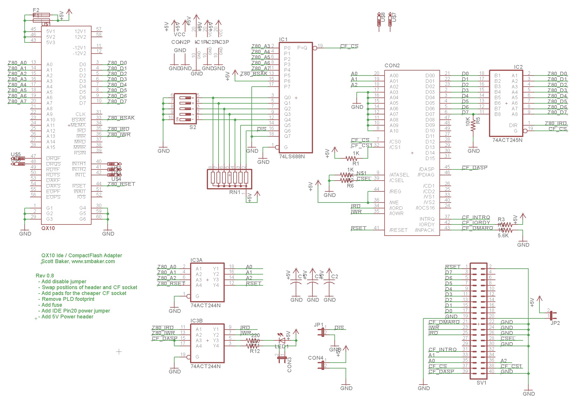
The schematic is fairly straightforward. There’s a 74HCT245 that is used as a data buffer, and a 74HCT244 that is used as an address and control buffer. Address decoding is performed by a 74HCT688. The dipswitches should be set so the first switch (corresponding to A7) is “Off” and the remining switches are “On”. This will correspond to address 0x80. Addressing is only enabled when BSAK is high. Both a compactflash socket and a standard 40pin IDE connector are wired.
Implementation
The second revision I produced, 0.10, is pictured below:
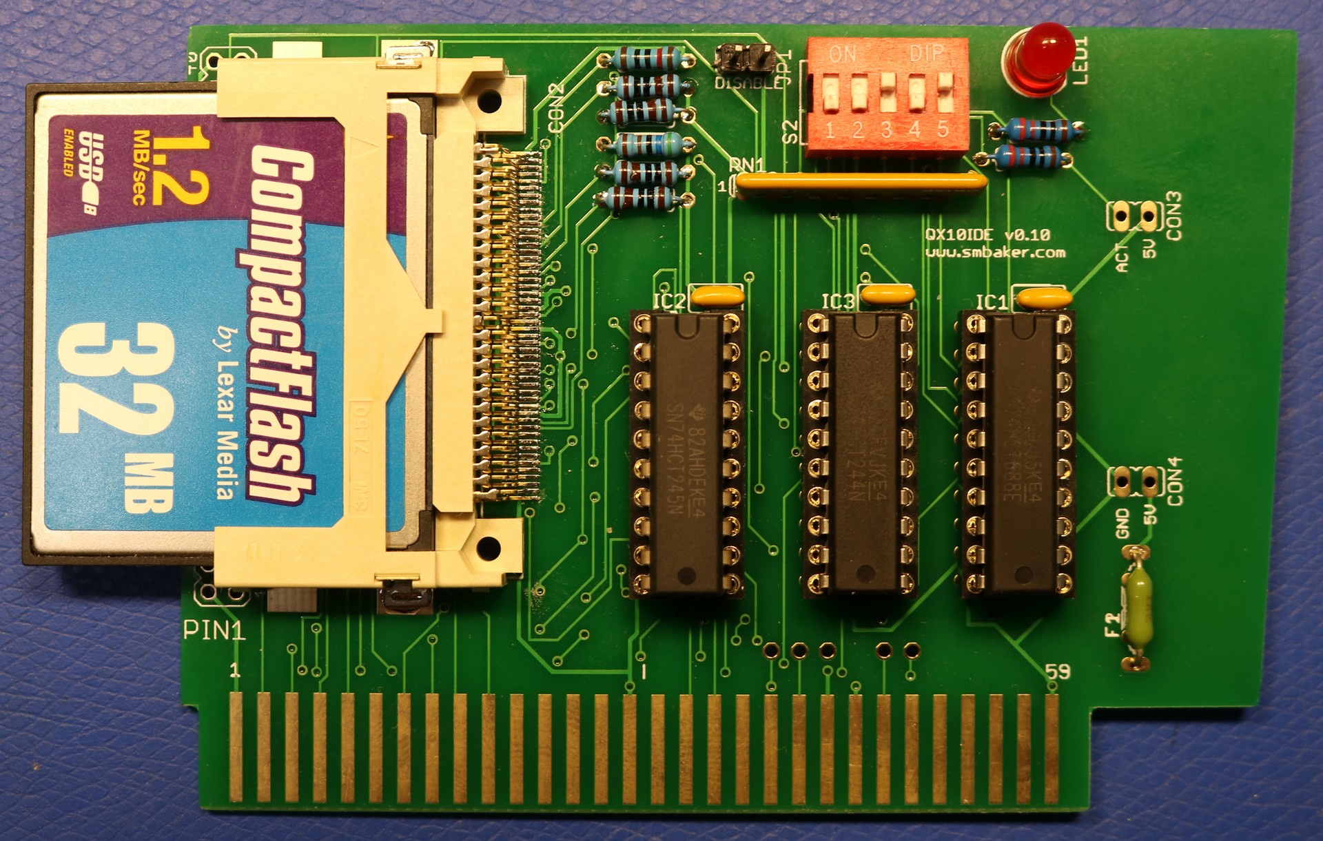
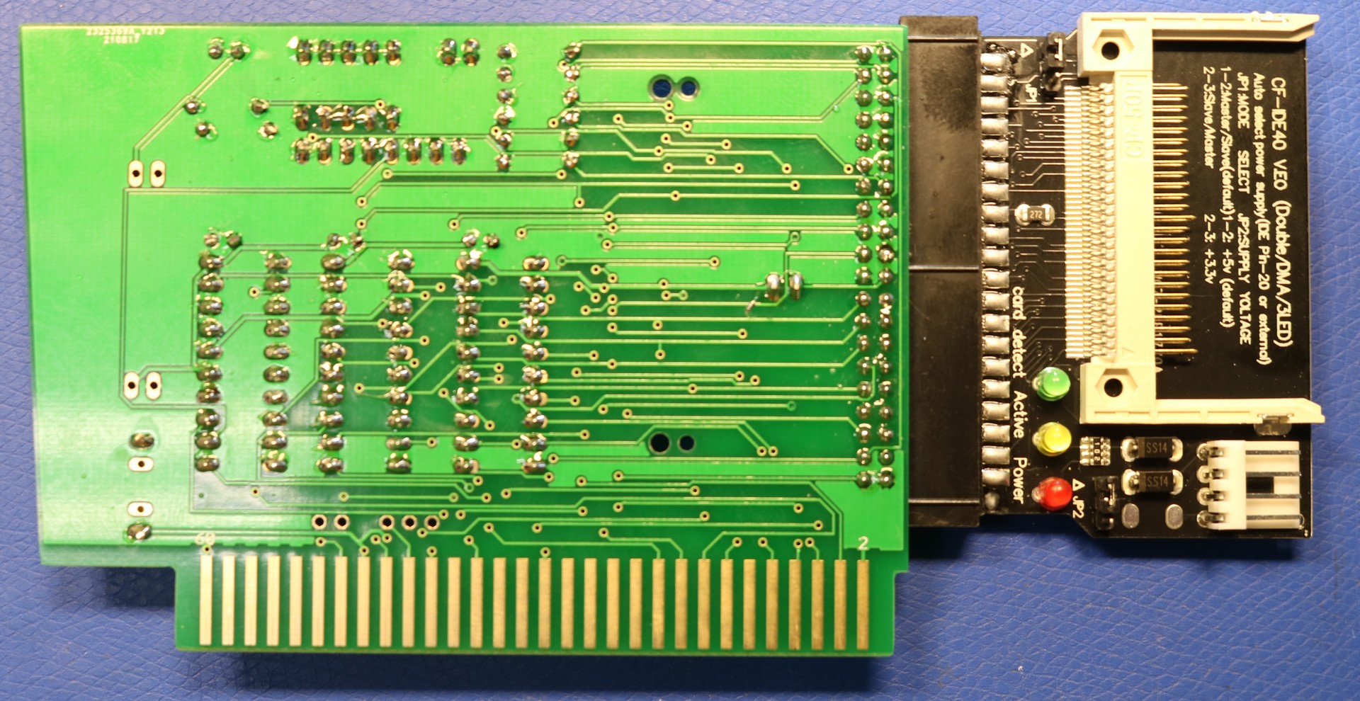
There are two ways to build the board. The first is by soldering an SMD compactflash socket directly to the pcboard, as pictured above. This is by far the cleanest implementation. However, the compactflash socket has very fine pitch, and may be a struggle for some people to build. So I also included the option of using a commodity SD-Card to Compactflash adapter, which can be purchased on Amazon:
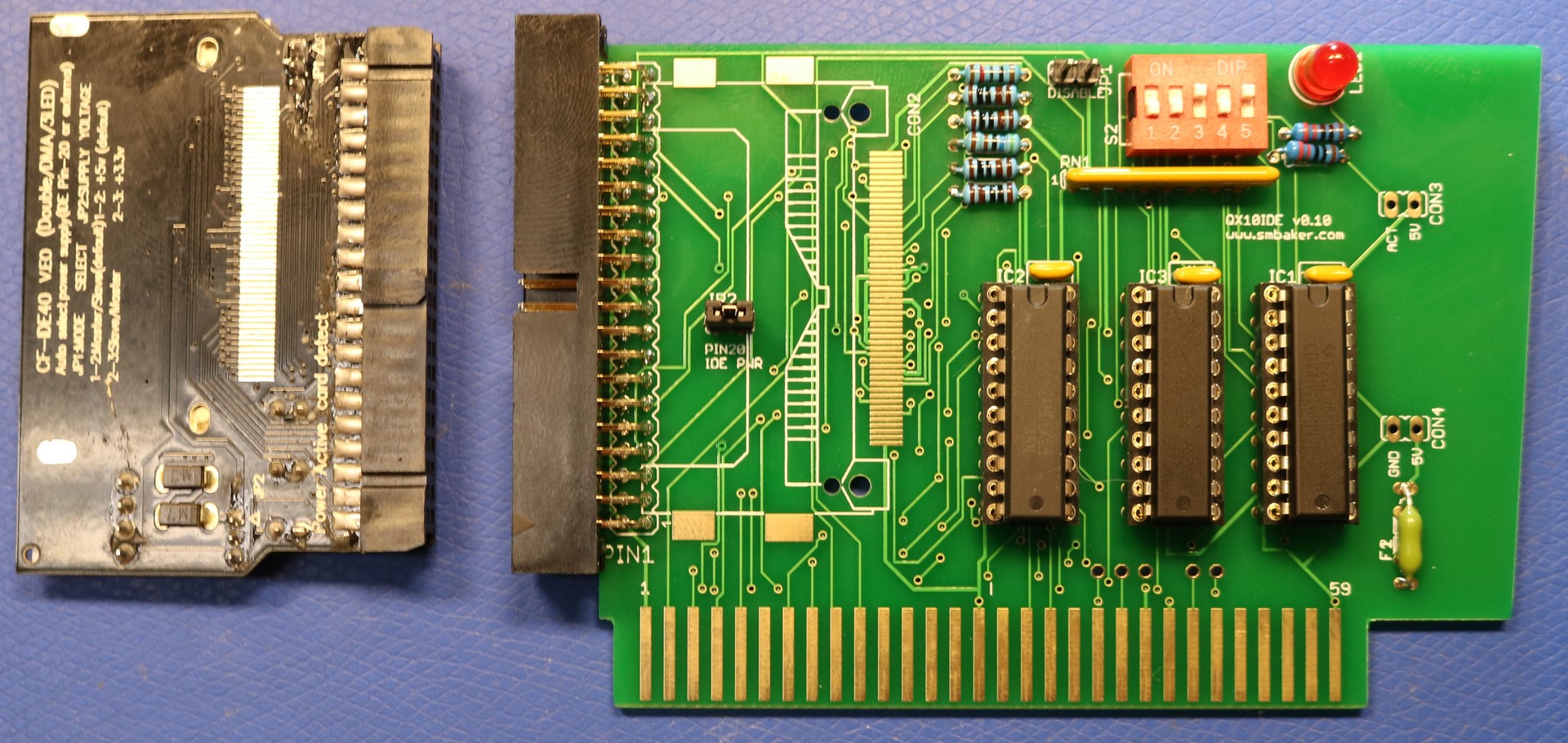
Note the above jumper JP2 is installed, this provides power to the IDE connector on PIN20, and is necessary to power the adapter board.
Also note that the module I found on ebay mounts upside-down:
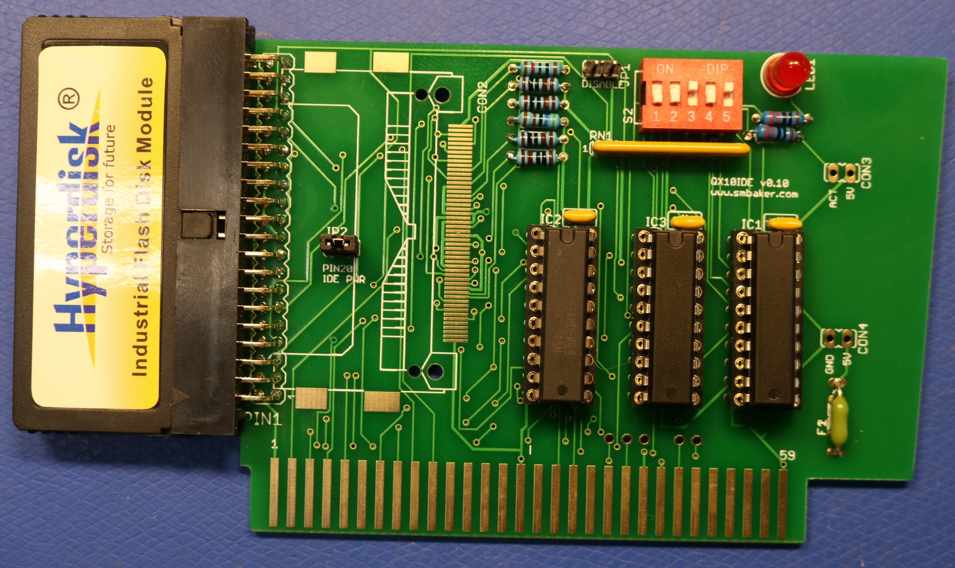
Instead of a compactflash, you can also use a “Disk on Module” (DOM). The DOMs were typically sold for industrial applications and may be more durable than a compactflash device. Here’s an example:
In all of these pictures, please note the DIP Switches, which differs from my original video. They are configured (from left to right) as OFF-OFF-ON-OFF-ON. This places the IDE device at address 0xD0 in the QX-10 Z80 address apce.
Bill of Materials
| Symbol | Qty | Desc | Mouser Part |
|---|---|---|---|
| IC1 | 1 | CD74HCT688E Logic Comparator | 595-CD74HCT688E |
| IC2 | 1 | SN74HCT245N Bus Transciever | 595-SN74HCT245N |
| IC3 | 1 | SN74HCT244N Buffer/Line Driver | 595-SN74HCT244N |
| CON2 | 1 | N7E50-7516PK-20 CompactFlash socket (alternative: use SV1 with external adapter) | 517-N7E50-7516PK-20 |
| SV1 | 1 | 40-pin shrouded right angle header (optional alternative to CON2) | 517-30340-5002 |
| C1-C3 | 3 | 0.1uF Monolithic Ceramic Capacitor | 80-C320C104M5R7301 |
| F1 | 1 | 0.1A pico fuse | 576-0251001.MXL |
| RN1 | 1 | 10K 7 resistor sip | 652-4608X-AP1-103LF |
| S2 | 1 | 5-position dip switch | 490-DS01C-254-L-05BE |
| LED1 | 1 | 5mm Red LED | 604-WP7113SRDJ4 |
| R1,R2,R3,R6 | 4 | 1K resistor | 291-1K-RC |
| R4 | 1 | 5.6K resistor | 291-5.6K-RC |
| R5 | 1 | 10K resistor | 291-10K-RC |
| R11,R12 | 2 | 220 ohm resistor | 291-220-RC |
| JP1, JP2 | * | 0.100 header, cut to length | 571-9-146274-0 or ebay |
| JP2 | 1 | shunt | 710-60900213421 |
| 3 | 20-pin ic sockets (if desired) | 575-11043320 |
Tested CompactFlash and DOM devices
- Silicon Systems 32MB Compactflash: Good
- Lexar Media 32MB Compactflash: Good
- Wintex 128MB Compactflash: Good
- Hyperdisk Industrial 1GB DOM: Good
- Centon 32MB Compactflash: BAD – Locked up while writing partition table
Setup instructions
- Download the repository and burn
images/qx10ide.imgusing your favorite tool. NOTE: This image is 16 sectors of 256 bytes each for the first two tracks, and 10 sectors of 512 bytes each for the remaining tracks. This is relatively easy to setup using a custom profile for flashfloppy/gotek (my custom profile is in flashflop/img.cfg). - Set the dip switches to OFF-OFF-ON-OFF-ON. This will set the board to address 0xD0.
- Attach a compactflash device
- Insert the board into your QX-10
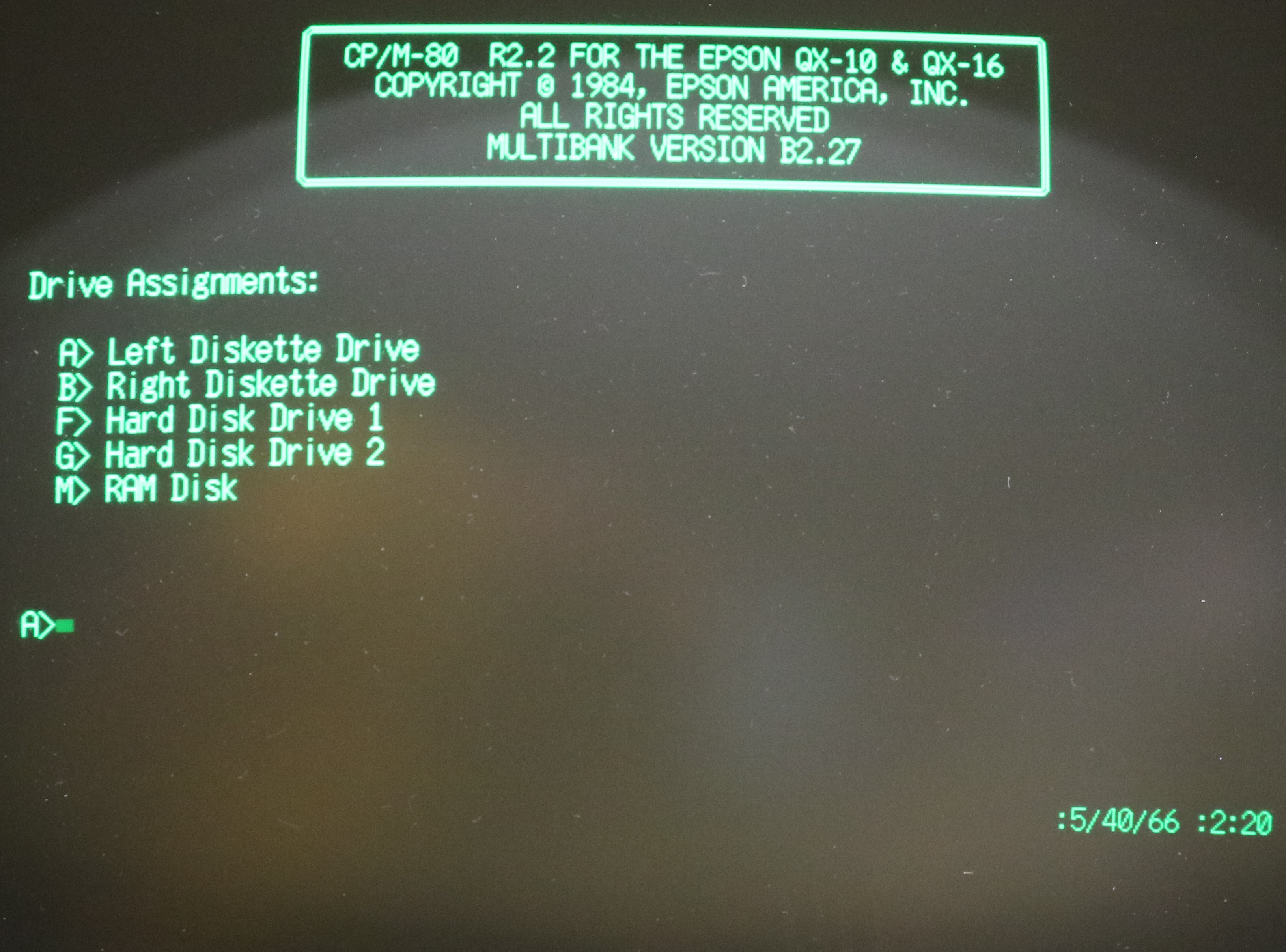
- Boot the custom image
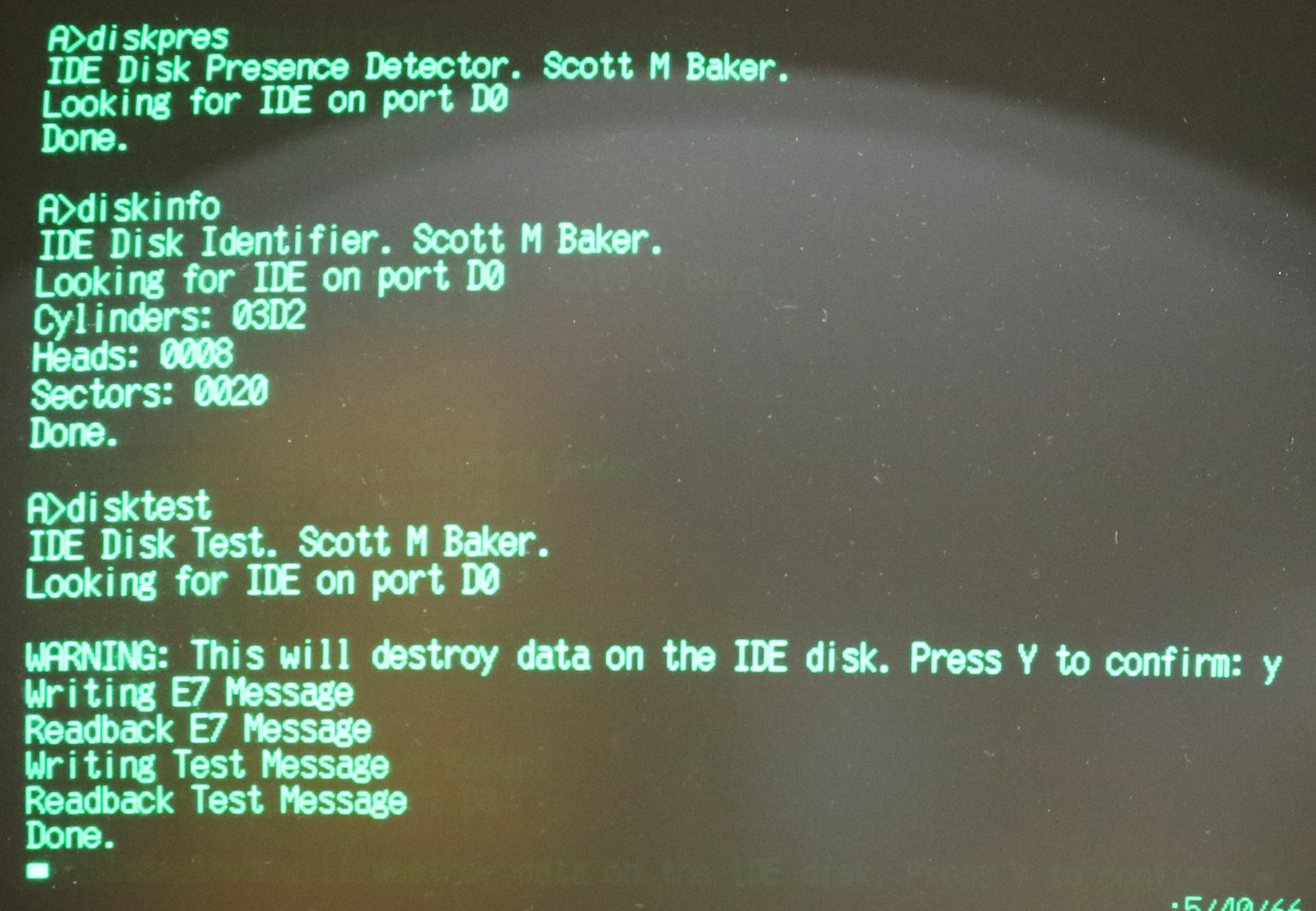
- Run DISKPRES.COM, this will verify the IDE device is detected
- Run DISKINFO.COM, this will print out some information about your flash device.
- Run DISKTEST.COM, this will write the first sector of your compactflash and read it back.
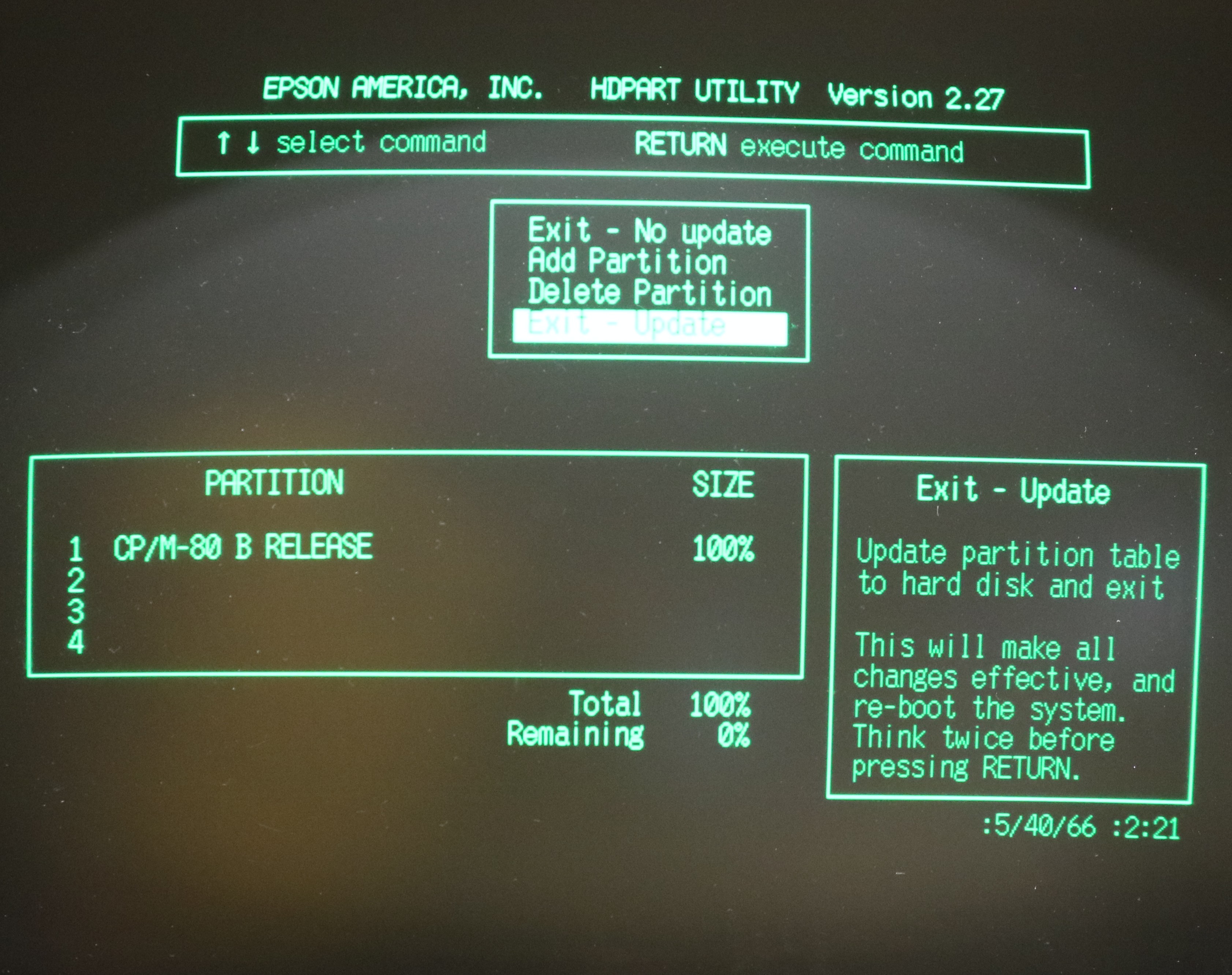
- Run HDPART.COM and create a CP/M partition occupying 100% of the disk.
- Reboot as instructed by HDPART
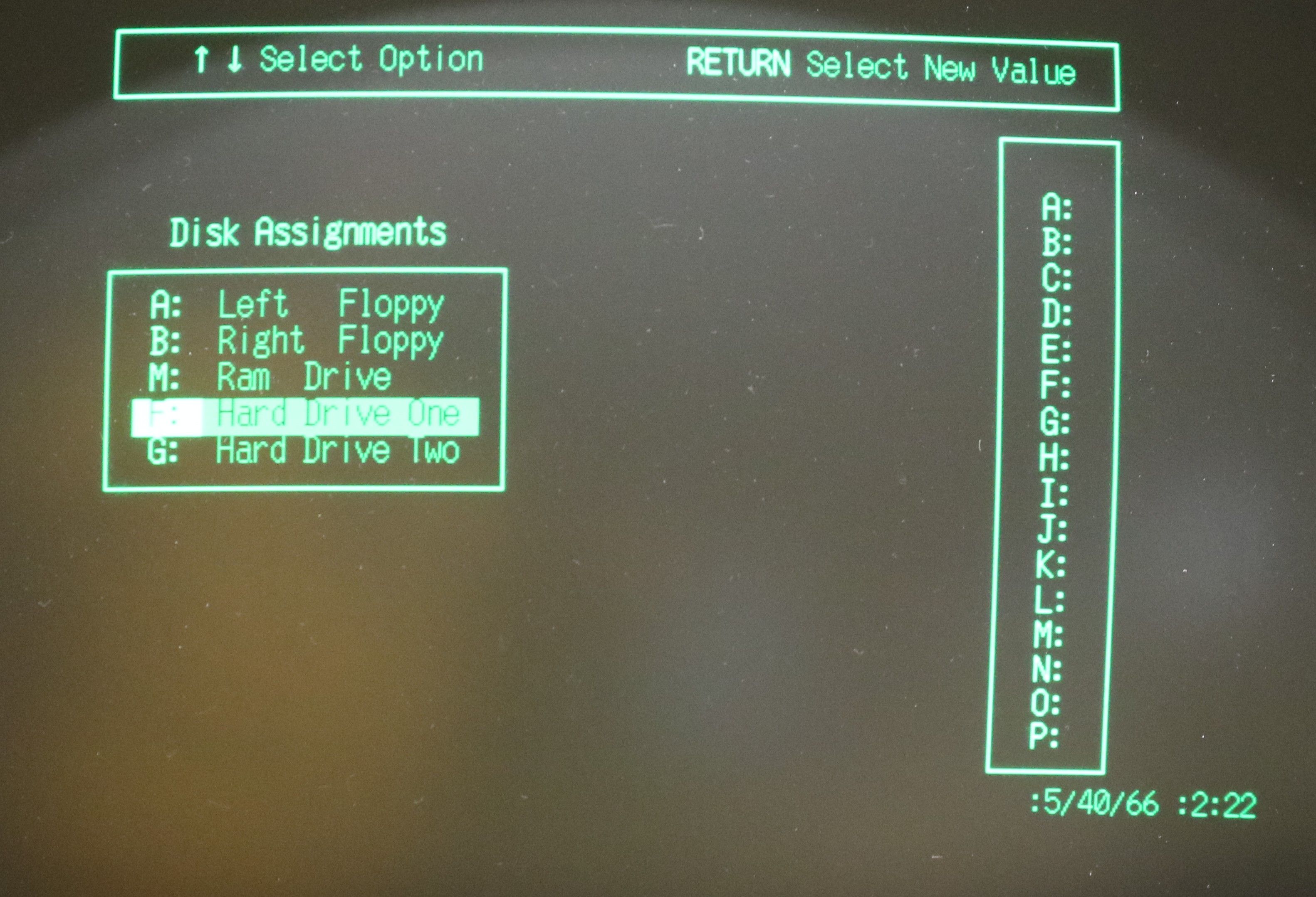
- Run SETUP.COM and assign drive letters to the two hard drives (the partition created by HDPART will be split into two equal virtual drives, so assign two letters)
- Reboot for changes to take effect.
Some screenshots of the above steps:
Resources
Here are some useful resources:
- https://github.com/sbelectronics/qx10 my github repository. The
asmdirectory contains patches related to the IDE BIOS changes, as well as a completed image (images/qx10ide.img) that can be booted. Note that this image file has 16 sectors of 256 bytes each for the first two tracks (on each side), and 10 sectors of 512 bytes each for the remaining 10 tracks.
Dear Dr Baker,
I was delighted when I visited your site yesterday & saw the two QX-10 projects.
I have been a fan of the QX-10 since I bought mine in 1982 or early 1983,. complete with a FX80 printer. Later I even bought the Hayes 300 baud modem.
I loved the screen showing WYSIWYG & the intuitive keyboard in VALDOCs.
The down side was the constant floppy disk access – but I loved the “UNDO” button – & having to swap disks to change applications.
The cost of a Comrex Commfiler (?) hard drive was well beyond what I could afford at the time.
We had a Xerox computer at work (with 8″ drives) so I had to learn to use Wordstar – possibly quicker on the keyboard than VALDOCS but I had to have a keyboard overlay handly as I could not remember all the keystrokes. Also it was not WYSIWYG
So once we had an Amstrad PC1520 & bought a hard card, the QX10 was retired.
I would dearly love to build the CF/IDE adaptor board mentioned in your blog, to see how the QX-10 will run with a “hard drive”. Will you be selling these boards or would you be so kind as to let me have the Gerber files, please?
Did you ever try the TPM II & TPM III operating systems when VALDOCS ran on? Was supposed to be similar to CP/M?
The reason I ask as from your blog it looks like you have had to make some patches to the CP/M yet I would like to run VALDOCS with the IDE adaptor.
Just for the fun of it I am also interested in the sound & speach cards you made for the the QX-10. Would you be able to send me the Gerbers for these board too, please?
I am curoius as to where you got the software for your QX-10 from – as most of my disks are probably no longer usable – being around 30 to nearly 40 years old.
Thank you very much.
David Williams
Australia
Thank you for developing the QX-10 IDE controller card – a very useful addition! While watching the video I noticed your floppy disk emulator. Can you provide any information about how you added the Gotek floppy emulator to your QX-10? Are there specific models of the Gotek unit that are needed to work with the QX-10? Thank you for any help you can provide about this (and also for your many years supporting older computers) – that has been a huge help! I am working to bring a QX-10 back to life and your video’s have been a real encouragement! Rick