In this post, I build a Basic Flash and RAM board the the HP 9000 series of computers:
Purpose
Lately I’ve been playing with old HP computers such as the 9836, 9920, and 9000/310. These computers typically do not come with ROM basic or any other ROM operating system. Without a ROM board, you have to boot off disk, either a floppy or an attached hard drive. There were ROM boards back in the day, but if and when you encounter them on eBay, they can be pricey. So I decided to make my own.
Background / Research
I started by looking around at the HP Museum, and found references that Dominique Berget had documented the schematics and reverse engineered and reproduced the Basic 4.0 board. I contacted Dominique and asked him a few emails — he sells completed boards, but not kits or bare pcboards. He provided me with some additional schematics, links to the ROM images, and advice on creating my own board. It seemed simple enough to do so, so I set out to design and fabricate my own boards. While the first one more-or-less worked, it took me about four revisions to finally get the design to the point I was happy with it.
The HP Dio Bus
The Bus used on the HP 9000 200 and 300 series is called “DIO”, and you can find some specifications for it on the web, including even schematics for how typical memory and peripheral boards are implemented. Typically, an expansion board buffers everything — 74LS244 buffers are often used for unidirectional signals such as address lines, and 73LS245 buffers are used for bidirectional signals such as data lines. The bus is 16-bit, and includes a pair of signals, BLDS and BUDS that tell you whether to read/write the upper or lower 8-bits. Reading or writing both the upper and the lower 8-bits at the same time is common, especially for memory boards. There is an IMA signal that is used by the expansion board to indicate that an address has fallen into the board’s address space, and a DTACK signal that indicate when a transfer is complete.
Designing a ROM, Flash, or RAM board is as simple as the following:
- Buffer all of the address bits.
- Decode the address to determine whether your board is addressed.
- Assert the appropriate data buffers for lower or upper transfers, and set them to the proper direction (read or write)
- Assert IMA to indicate that you board is handling the request.
- Transfer the data
- Assert DTACK when you’re done.
In my experience, DTACK is where all of the complexity comes into play. There was actually a movement back in the day, “DTACK Grounded” that asserted you could simply ground the line, and if memory was fast enough, everything would just work. I’m not sure if this would work on the 9000, but to do it to spec needs some additional work.
- Some computers, the 9836 and 9920, will automatically assert DTACK for you, for some addresses. More than anything I found this a bit annoying, as it complicates the implementation (which computer do I have? Is my board outside the auto-dtack space or inside it?).
- There’s an ENDT (“Enable DTACK”) line asserted by the processor that you can use. If your card is selected, then you can simply pass ENDT through to DTACK, and you will end up asserting the DTACK about 5 cycles into the transfer.
- However… if you have a DMA board such as the 98620A or 98620B, the DMA board will perform memory transfers but it will not generate ENDT. The DIO specification says that every board that can accept ENDT must also work if ENDT is not implemented. For this reason, as a fallback you need to implement your own delay line.
Schematic
Below is the schematic for my board. Let’s go through it a page at a time. Click any of the schematic pictures to get a decent size view.
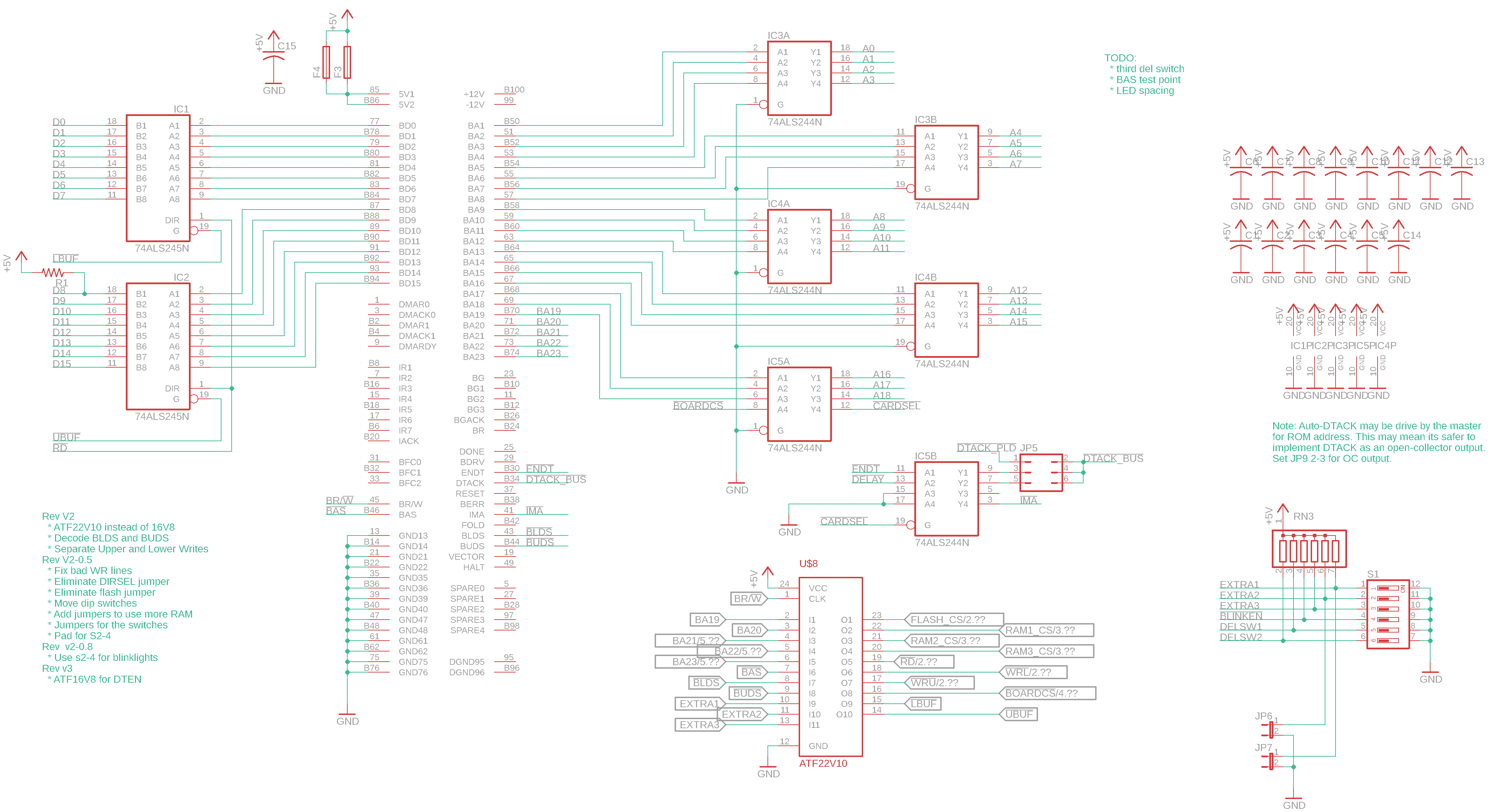
Above we have the standard buffering arrangement. There are two 74ALS245, one each for the upper and lower data bytes. There is a separate enable to drive each one of them, and a direction that is common to both of them. For the address lines, there are a plethora of 74ALS244 which are always enabled and unidirectional. There is half of a 74ALS244 left over, so it gets used to drive the IMA signal. The ‘244 is a tri-state device, when it’s not enabled IMA can float. When the device is enabled, the ‘244 will drive IMA low. This half of the ‘244 also gives us our first option to implement DTACK — by selecting the second position of JP5, we can drive DTACK based on ENDT. By selecting the third position of JP5, we can drive DTACK based on a delay. Don’t try to use both positions at the same time — we’ll get to that later.
An ATF22V10 handles all of the decoding logic. It decides when the board is addressed, which RAM or Flash chips to select, when to enable the upper or lower buffers, etc. This device needs to be programmed, and can easily be programmed with a TL866II. Note that the original TL866 will not program the ATF22V10.
The next page is for the Flash ICs
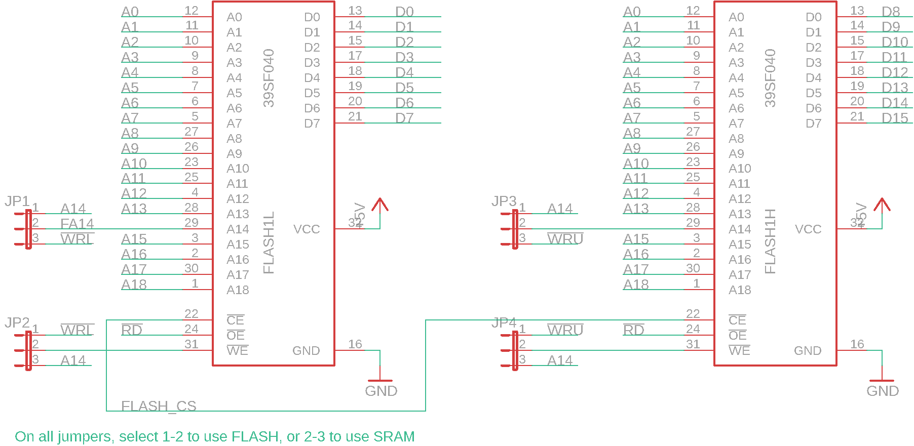
The above is simple enough, it’s just two 39SF040 flash memory ICs. Recall this is a 16-bit bus, so to use 8-bit memory devices like the 39SF040, we’ll need two ICs, one for upper and one for lower. The four jumpers allow you to switch these sockets between the pinout for a 39SF040 and an AS6C4008 memory IC. The pinouts of those two devices are almost identical, but annoyingly not quite identical. By moving the jumpers, you can change the board from a hybrid flash + RAM board to a board that implements all RAM. Next up are the RAM IC sockets.
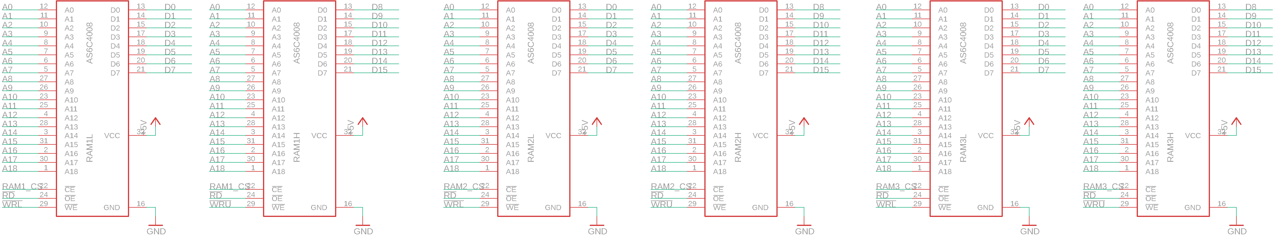
The RAM sockets look much like the Flash sockets. There’s 6 of them, 512KB each, for a total of 3MB. Again note that the upper and lower ICs are selected separately. Next let’s have a little fun!
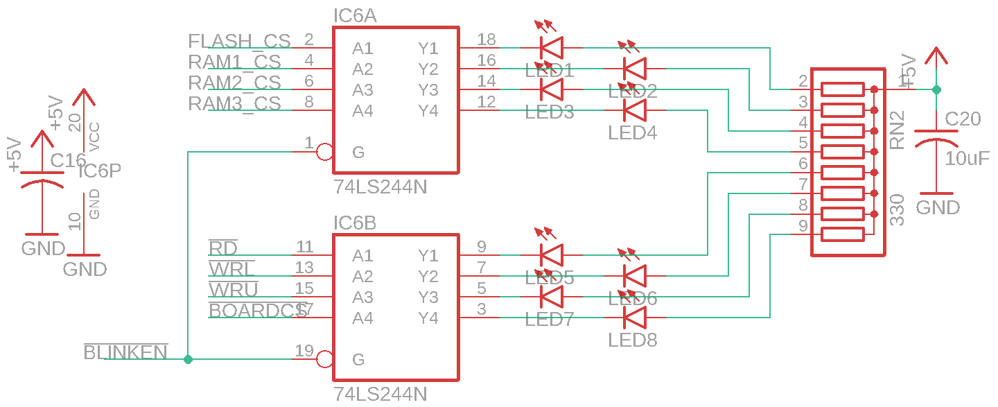
Everybody likes blinky lights! Here I used another 74ALS244 IC to drive the LEDs. They’re connected to the chip selects for each of the memory backs, the RD and WRT strobes, and the board chip select. The lights aren’t merely frivolous; I did use them to diagnose the earlier versions of the board. When the computer is booting and doing the memory check, you can see each of the CS lines light up in turn.
Finally, one last bit of complexity…
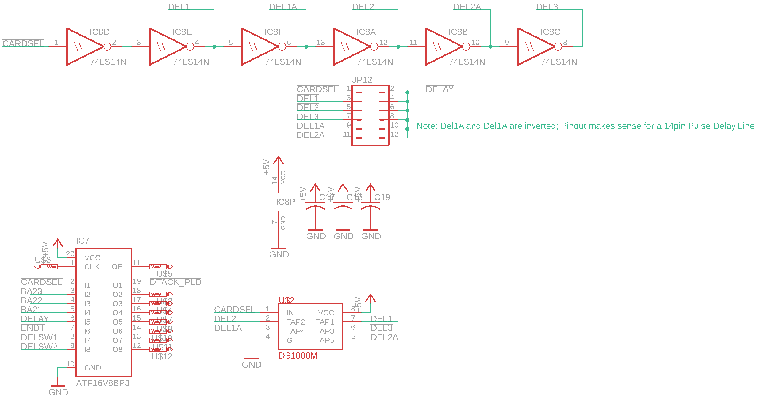
As I mentioned previously, the DIO specification insists that using ENDT to trigger DTACK is not sufficient. Every board must also be able generate DTACK even if ENDT is never asserted. This is necessary to function correctly with the (optional) DMA board. There’s also the nit about AUTO-DTACK, that the computer may be asserting DTACK for certain addresses.
For this, I added another PLD, this time a slightly smaller ATF16V8. The primary function is as a fancy OR function — it can assert DTACK if it sees ENDT asserted, or it can assert it after a fixed delay. The ATF16V8 can be configured to support a tri-state output, which is perfect for the bus specification. Finally, it also pays attention to the upper 3 address bits and can be configured to avoid asserting DTACK in the range where it thinks the CPU will be doing auto-DTACK.
To generate the actual delays, I used a 74LS14N schmidt trigger inverter. This device has a relatively reliable delay of about 15ns per gate. If you put jumper JP12 in the second position, you should get about 30ns of additional delay. If you put it in the third position, you’ll get about 60ns of additional delay. However, in my tests, I found that using the 74LS14 was not necessary — there was sufficient delay already in the other logic circuits (the ATF22V10, the 74LS244 buffers, etc) that I was able to jumper JP12 in the first position, which is zero additional delay. That would be my default suggestion — leave IC8 unpopulated and put JP12 in the first position. If it gives you trouble, then populate IC8 and move the jumper to the second position.
U$2, a DS1000M was an alternate footprint for an alternate purpose-built delay IC. They’re not made anymore, but some can be found on eBay. Ultimately it was not necessary and can be safely ignored.
Implementation
Below is a picture of the board.
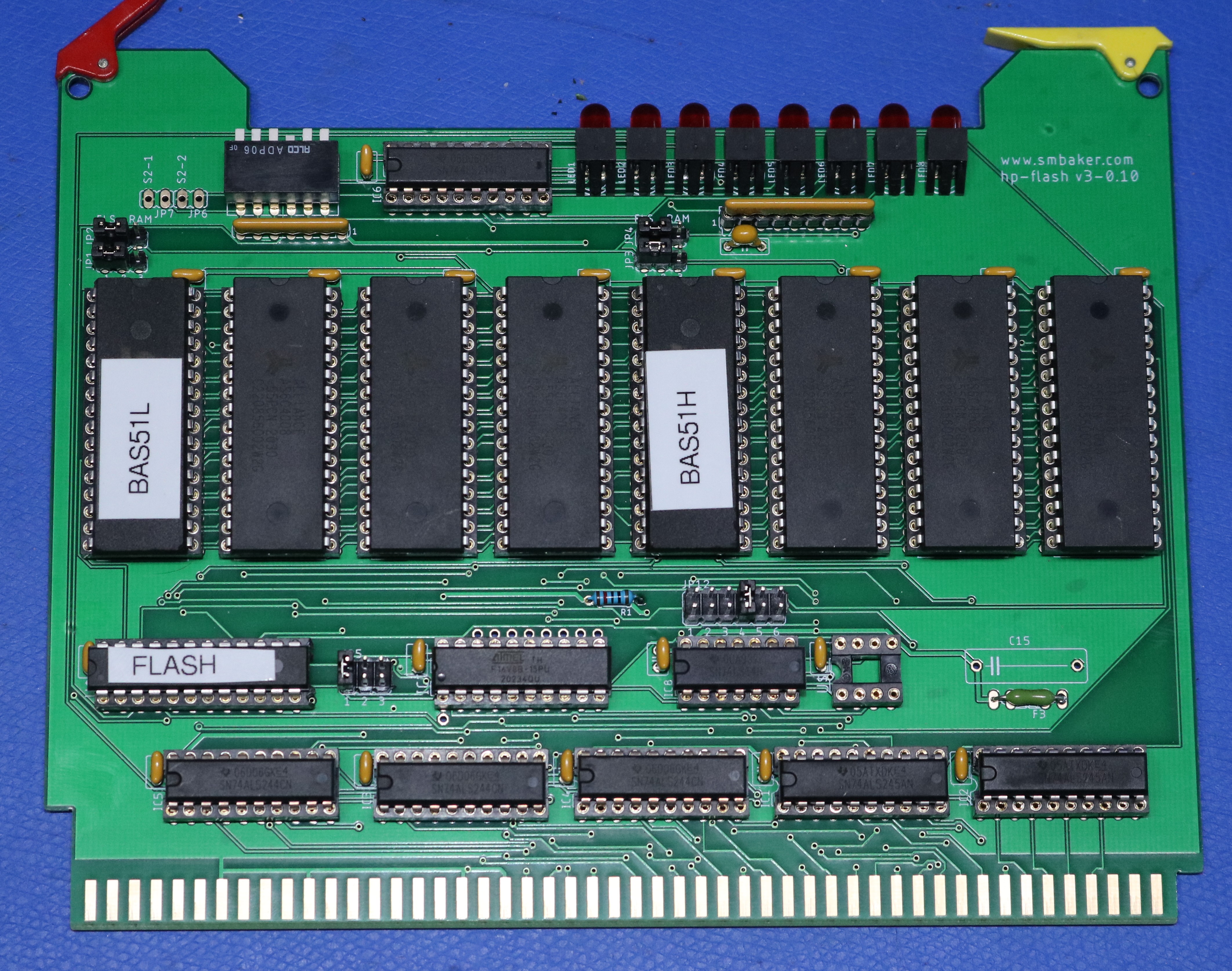
The implementation is rather straightforward — above you can see the two flash ROMs with white labels on them, BAS51L and BAS51H for lower and upper respectively. The other large ICs are the RAM chips. The 22-pin narrow DIP is the PLD device. JP12 is in the 90ns delay position; this photo was taken before I realized I could jumper it to the 0ns position.
I opted to go with a right-angle dip switch. This makes it easy to adjust the board while it’s mounted in the case. The little red and yellow ejecter levers were scavenged from a 256K HP RAM board.
Resources
TODO: Work in progress… Put up the github repo link…
Thanks – at first I was worried that you wouldn’t be sharing the nitty-gritty. Looking forward to seeing more on github.
Hi Scott: I built a board for each of my HP-9000 Series 300 computers. I have also tested the board in a 9000 Model 216 (aka 9816).
They work wonderfully! Many thanks! Juergen