In this video, I build a DC electronic load that’s controlled by a raspberry pi.
Purpose
A DC Load is useful for testing lots of different things. If you have a power supply and want to make sure it’s able to deliver its fully designed potential, then you can use a DC Load to test that power supply. If you have batteries and you want to know if they’ll provide their rated capacity, then a DC Load can tell you that. I’ve also used a DC Load for testing USB cables to see which cables perform the best. There’s a lot of possibilities, and it’s a useful piece of test equipment.
I’ve built a few DC Loads before, and I even own a commercial unit, a Kunken KP184. So why build my own? Well there are a couple reasons:
- I like raspberry pi based projects, because the pi is a great platform to roll out a web server that can be used to operate the project from a desktop PC or a mobile device. There’s the opportunity to build in data logging or graphic, or to set up custom ramp features for testing devices.
- Building the load yourself allows you to select the MOSFETs and pick a voltage/amperage range that works for you. Sometimes I work on high voltage projects and having a range that goes into the hundreds of volts may be useful.
- It’s a challenge and a learning experience. Even when you think something is simple, sometimes unforeseen complications arise and need to be worked through.
Let’s start with a basic Analog Load
The basic analog load design I picked up from an old EEVBLOG post and have been using it in my projects ever since. Here’s a schematic:
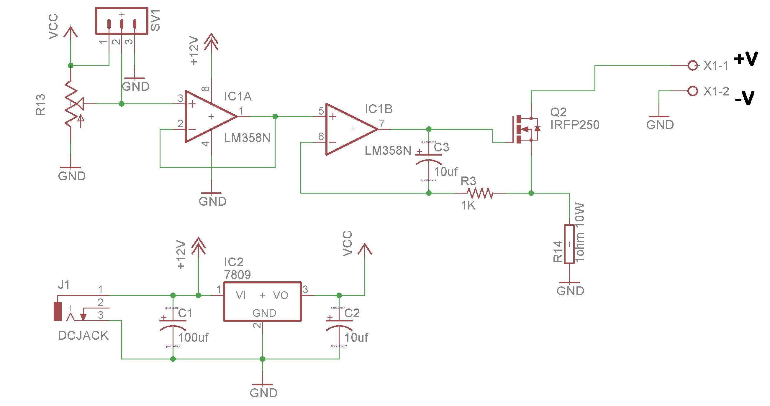
The basis of this circuit is ohm’s law. A 1 ohm current sense resistor is used to sense the amount of current that is passing from the +V to -V terminals. A 1 ohm resistor with 1 amp of current will drop exactly 1 volt. If you measure the voltage on each side of the resistor, you can easily compute the amount of current.
On the left side of the schematic we have a potentiometer and a unity gain op-amp. The unit gain stage isn’t strictly necessary, but we have a spare gate in the op-amp, so why not use it. This potentiometer gives us a variable voltage that ranges from 0V to 9V. That will be our setpoint.
The setpoint and the measurement from the current sense resistor are fed into the second gate of the op-amp. Now, when you feed an op-amp two inputs, it’s going to try to make them equal. If the current sense input is less than the setpoint, the op-amp will turn its output on. If the current sense input is greater than the setpoint, the op-amp will turn its output off. So what we have is a circuit that’s constantly evaluating it’s input and producing and output that attempts to equalize them.
The remaining component is a large power MOSFET. When you supply a gate voltage to the MOSFET, it’ll turn on and start conducting. The MOSFET conducts, completing the circuit through the current sense resistor. The more you turn the MOSFET on, the more current will flow through the resistor and the higher the resulting sense voltage. The less you turn it on, the lower the current and the lower the sense voltage.
This is a simple circuit that can often be built from parts sitting in your junk bin.
Note that C3 and R3 are something I haven’t included in my previous designs. They serve to dampen the oscillations of the circuit. Without these two components, the circuit will start to oscillate wildly about the setpoint at certain amperages.
Adding more MOSFETS
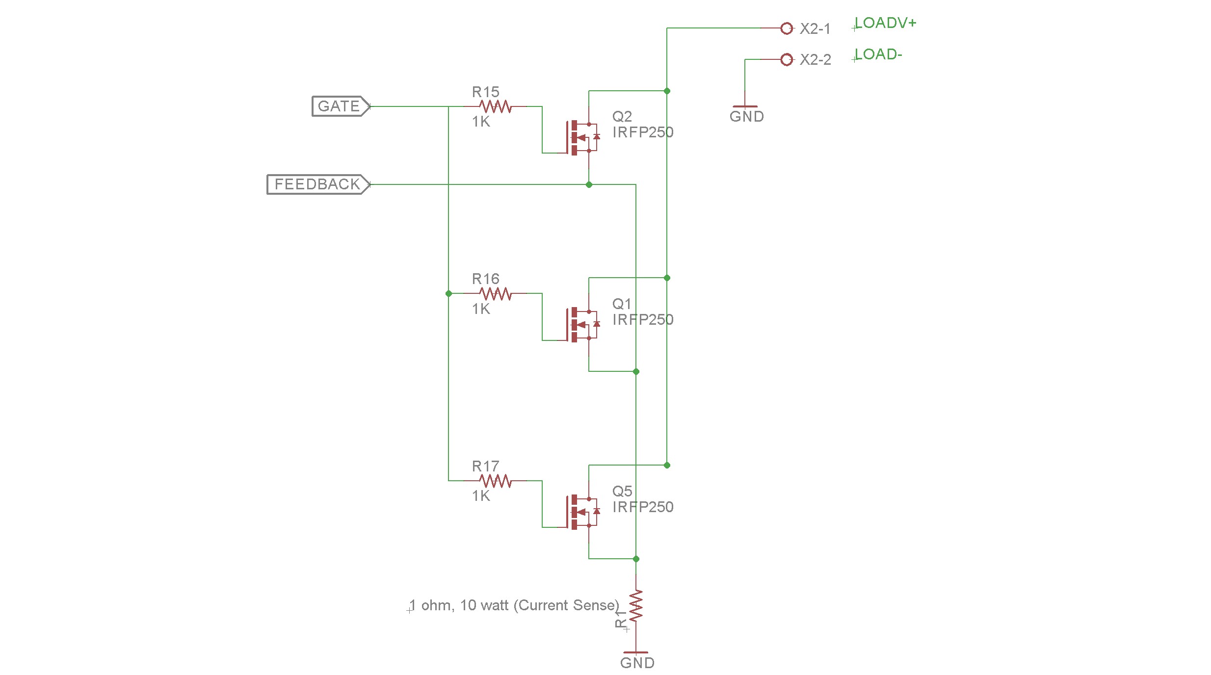
We’re going to take a little detour and talk about adding additional MOSFETs to the circuit. Why do this? Because a single MOSFET can easily be overheated. These components need to shed a lot of heat. Adding a few in parallel will be safer than a single MOSFET. In theory as a MOSFET heats up, it conducts a little less, and its load will shift to a cooler MOSFET. In theory this causes some equalization between the MOSFETs. I say “in theory” because there often seems to be some temperature differential between multiple MOSFETs in parallel.
You’ll also want to add some gate resistors to the MOSFETs in order to dampen oscillations between them:
A computer-controlled DC Load
This is really going to be pretty simple. We’re going to drop the Potentiometer and put a Digital to Analog Converter (DAC) in its place.
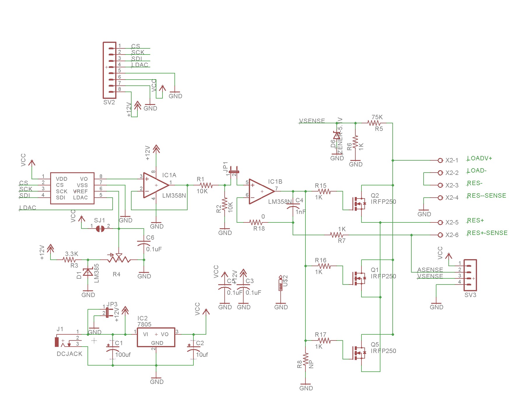
So you’ll see the potentiomer is gone and we now have an MCP4821 (or MCP4921) digital to analog converter in its place. This is a 12-bit DAC, with 4096 possible values. The 4821 has an internal reference, whereas the 4921 has an external reference. All else being equal, the 4821’s internal reference makes it easier to deal with, and fewer components. I went with the 4821.
The DAC connects to the pi through 4 control lines: CS, SCK, MOSI, and LDAC. The first three pins (CS, SCK, MOSI) are all SPI bus signals and are connected to the appropriate SPI pins on the pi. LDAC is used to latch the data value into the DAC. I think you can wire it to ground, but I chose to wire it to a pin on the pi. So controlling this is pretty simple — you write a value between 0-4096 to the DAC, and it outputs a value between 0 and 4.096 volts. That is our setpoint instead of the potentiometer.
You might notice the current sense resistor is missing from the above schematic. It’s not gone — it’s just been moved externally. An external resistor means we can use a ginormous metal-clad resistor that can dissipate a fair amount of watts.
You might notice that there are four wires connecting to the current sense resistor instead of two. This keeps the patch where the current flows separate from the path where the voltage drop is measured. At high loads, those external wires can drop some voltage themselves, and not having the additional measurement wires would lead to a little bit of additional resistance and additional error in the circuit.
Not evident in this schematic is that for the load I built I switched the current sense resistor from 1 ohm to 0.1 ohm. Instead of 1A = 1V, that gives us 1A = 0.1V, which means we could scale this circuit all the way up to 40A ( = 40V) if we wanted to. The disadvantage of using the 0.1 ohm resistor is a resulting lack of precision. We still only have 4,096 steps on the DAC, and now we’re dividing those steps across 40 amps instead of 4 amps. Each step ends up about 10ma.
A separate header is provided for feedback to the pi, and has “asense” (for amp sense) and “vsense” (for volt sense) pins. This lets you confirm the voltage and the amperage. The pi doesn’t have analog inputs, so I used an ADC1115 (4 channel 16-bit ADC) on a separate daughterboard. The ADC1115 uses the I2C bus to talk to the pi.
We can both command an amperage (using the DAC), and readback the actual amperage (using the ADC).
Implementation
I have a pcboard fabricated at jlcpcb. It actually took me a couple of tries to get it right — my first prototype had some errors and I have to make a separate board for the final design.
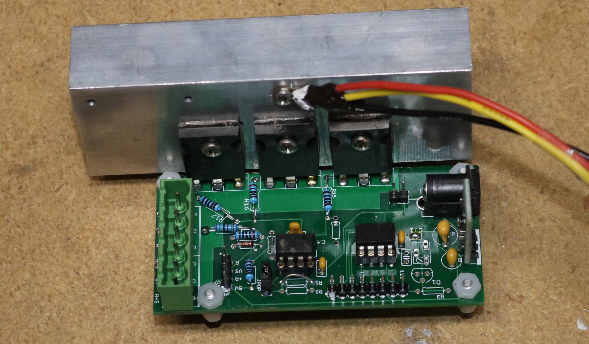
You can see a relatively small heatsink connected to all three MOSFETs. This heatsink, together with a 60mm Noctua Fan is good to about 100 watts. I used thermal grease between the MOSFETs and heatsink, but no insulators. The way the MOSFETs are constructed, the back of the MOSFET is metal, and is connected to the source of the DC Load. This means if you supply the load with 100 volts, that heatsink is live with 100 volts. Don’t touch it. Make sure it is either insulated from the project box, or that a non-conductive (plastic) project box is used.
The large green header is a part of a two-piece terminal block.
You can see a device with some wire leads attached to the heatsink. This is a DC18B20 digital thermometer IC, which allows me to readback the temperature of the head sink, to monitor thermal performance. It can also be used to shut down the load if it starts to get too hot.
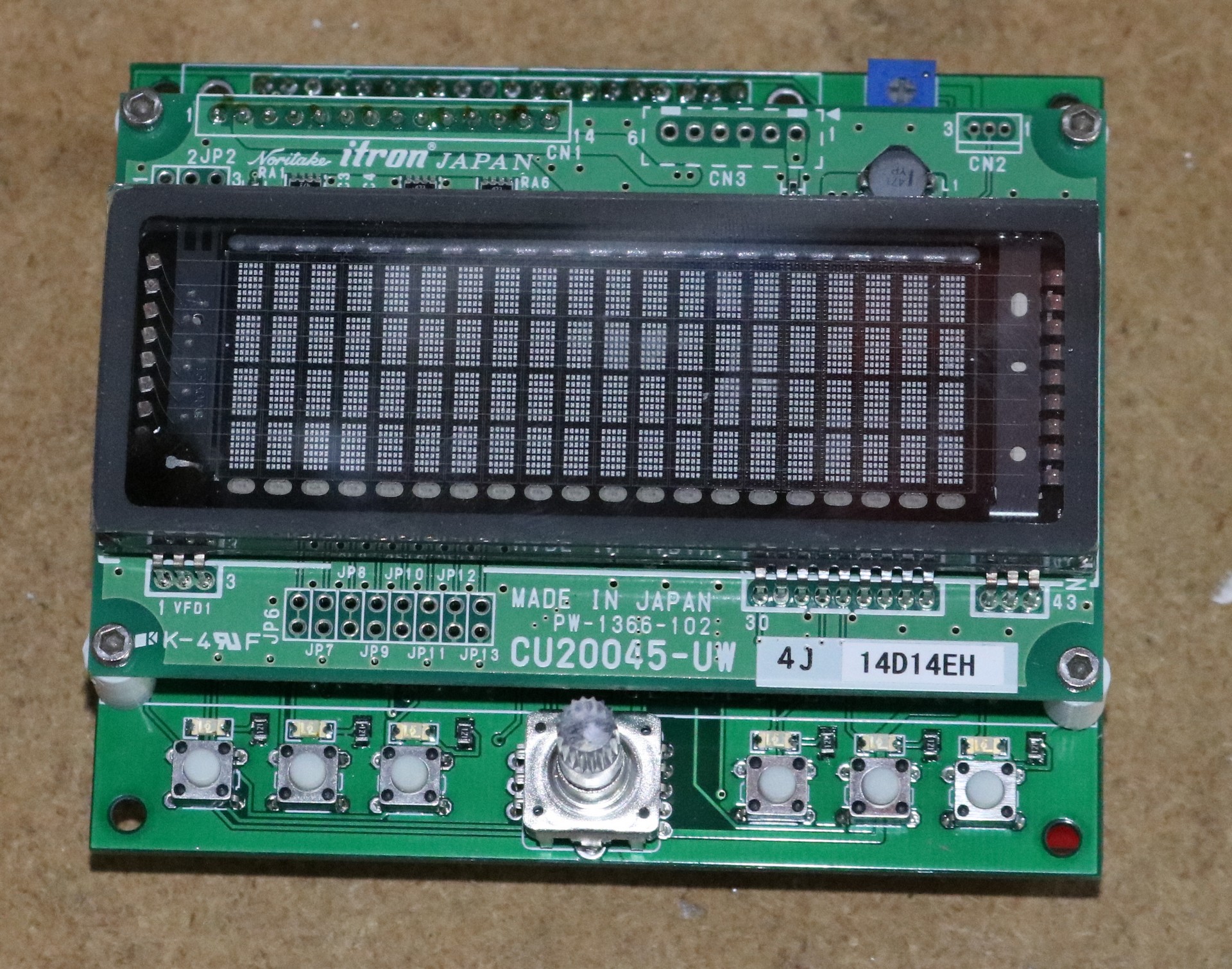
Front Panel
I implemented a front panel for the projects using a Vacuum Fluorescent Display, rotary encoder, and some buttons and LEDs. I’ll probably detail that front panel in a separate blog posts. It’s rather straightforward stuff (the VFD interfaces just like an LCD).
3D Printed Case
I 3D Printed a case:
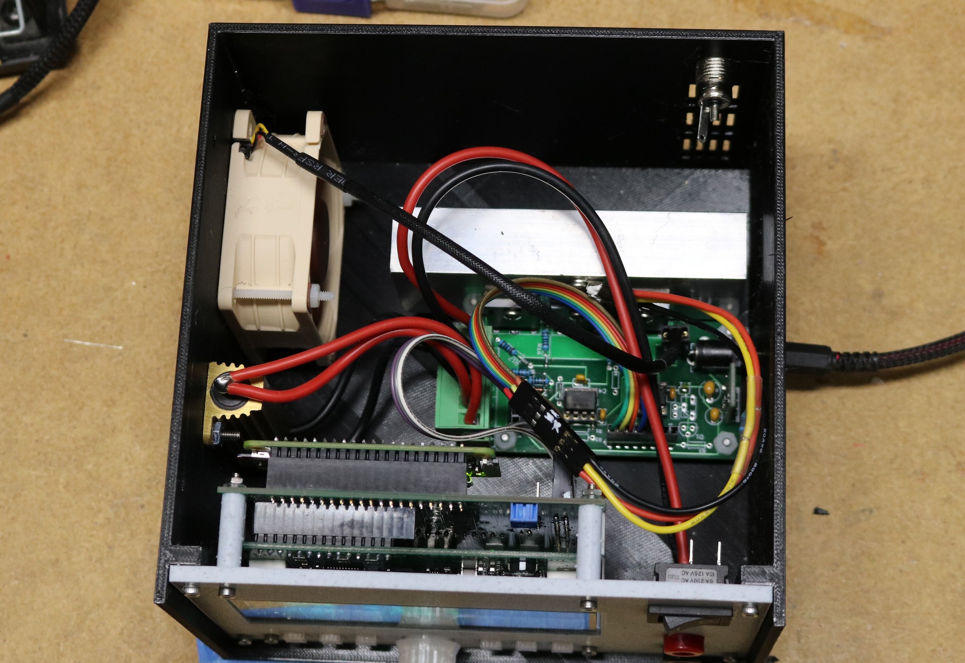
As you can see, there’s a lot of stuff crammed into that case. It’s printed in PETG, which should be good to about 80C before it starts to deform. Fortuantely, while the heatsink gets to around 75C, the case itself remains a bit cooler than that, so there is some margin of safety.
Software
The software is available on my github repository at https://github.com/sbelectronics/pi-dcload. It’s written in python and uses the django web framework to host a website from the pi.
Great Article… you have a really nice style of explaining things. I also appreciate how you even point out details such as what filament you used for the case.
So how do you deal with potential SD card corruption when powering down on projects that utilize the raspi?
Often I will put a button on the front panel (this project has 6 buttons, only 2 of which are currently used) that will print “Shutting Down” on the VFD and then initiate shutdown. I do like to try to be kind to the SD card. The other thing I typically do is:
1) Turn off swap
2) Mount /tmp, /var/tmp, /var/log, /var/run, and any other directories that might receive modifications during runtime to a ramdisk.
If you want to be really pedantic, you may even be able to remount root as readonly after doing the above steps.
A great project, I have been looking for connectors like the ones you used on the left-hand side for the sense resistor and load+, load-. Do you have any more information about them?