
DIY RF Signal Generator
It started out as a simple project, a DIY RF signal generator. Nuts and Volts magazine had two articles, in Dec 2013 and in June 2014 describing very similar designs. They used a MC1648 VCO chip along with a varacter diode to build a voltage controlled oscillator. This superficially worked out pretty well. I even produced a youtube video showing how my RF generator produces a variety of frequencies from 150 KHz to about 120 MHz. I took me around 5-10 hours to build this project.
Then, I started to do some detailed tests on it. The output is supposed to produce 2,000mv peak-to-peak, but I was only getting around 360mv peak-to-peak. The final driver stage of this design is a GALI-55 MMIC amplifier. I spent about 5 more hours poking and prodding the circuit before I cut the input dc cap of the GALI-55 loose from the rest of the circuit, attached my function generator to the input cap, and verified that the amplifier wasn’t working right. It wasn’t producing any gain. Something inside of it had fried. For further discussion, below is the relevant subset of the schematic:

GALI-55 schematic subset
I left out the value of C10 and C12 in the schematic as I’ve been playing around with those a bit. I’ve tried various values from 0.47uF to 0.01uF. Although my schematic above shows a polarized capacitor symbol, I’m using non-polarized ceramics. The datasheet indicates 0.01uF is appropriate for the bandwidth I’m using. R12 is a 392 ohm bias resistor. I’ve verified that R12 with a 24 VDC supply produces about 50 milliamps of current, consistent with the N&V article.
Figuring I must have somehow damaged the original GALI-55 during construction, I carfully replace the GALI-55, reconnected the circuit and it promptly failed again. Here’s a picture of one of my dead GALI-55:

One of the many GALI-55 that I destroyed
I replaced it again, but left the input disconnected and substituted my function generator and my bench PSU. Woohoo! the GALI-55 was working, producing about a 10x gain. I disconnected the benchtop PSU, reconnected the project’s built-in power supply. The GALI-55 failed.
I decided I’d prototype the GALI-55 on a breadboard. It worked using my benchtop PSU. It worked using the project’s power supply. At some point while I was switching power supply leads, the GALI-55 mysteriously failed. I don’t know why. I’m not sure what I did. At some point it just went from working to not-working.
Although the GALI-55 is supposed to have transient spike protection, I figure maybe it’s still getting some chip-killing transient spike from hell. I have the bright idea of putting a 5.1v Zener on the GALI-55s input power to ground. 5.1V is still beyond the device’s operating voltage, but I figure it ought to be good enough to stomp out any really nasty transients, and the chip’s on-board transient protection can handle the rest. I breadboard this out. I poke, prod, make a point of carelessly attaching and unattaching power leads. Switch the PSU on and off. I do everything I can to abuse the chip. It appears to be working just fine. Here’s what the revised schematic looks like:

GALI-55 with Zener protection added (don't do this -- it was a bad idea)
Satisfied that I had identified a transient spike issue and solved it with a simple junk box zener died, I added the zener to my PCB, soldered in a new GALI-55, and powered the project up. Here’s what my modified PCB looked like:

My PCB with zener added
It produced about 4X gain instead of the 10X gain it’s supposed to. Then at some point while I was fidgeting with the controls, it spontaneously failed.
I try different DC blocking capacitors in case that’s the problem. I keep frying GALI-55 MMICs.
Somehow I find myself tonight with only one GALI-55 MMICs left. I had originally ordered ten of them. Nine of them have now passed into the semiconductor afterlife. At this point, I’m at a loss. I don’t want to risk my sole remaining GALI-55 chip. I have an ebay order on the way from China with another 10 of them, which I’m sure I will promptly destroy if and when they arrive.
The morning after
Robert Reed, the author of the Nuts and Volts article, was kind enough to respond to a request I sent for clarification on the output stage with some tips, and I decided to start poking around the circuit the next morning. I attached my scope probes to the PCB, the one with the ‘dead’ GALI, just to get a baseline before desoldering it and installing my remaining good GALI. Turned on my signal generator.
The board worked. 10X gain just like it should be. The output waveform looked a little bit wonky, but the circuit is actually doing what it should be.
What?!? This was one of the GALIs that I was absolutely certain I had fried. The signal is doing an abrupt ‘clamp at 5.1v’ behavior so I cut that silly 5.1 Zener I put in there back out of the circuit. Strangely though when I move my multimeter probe near the circuit, it starts to misbehave and enters the same 1X-2X gain ‘bad state’ that I had been observing the prior night. It does this until I power cycle it, then it starts to behave again.
I take the board out. Put it under my microscope, look at everything real close and can’t find any loose connections, poor solder joints, etc. I though up a few of the pads. Hook it all back up, and … I can’t reproduce the ‘good’ behavior. It’s stuck in the 1X-2X gain state all the time now. I fuss with the probes. Make sure everything is good.
I write Robert again with my confusion, particularly the bit about the circuit misbehaving when I move metal objects near it. He thinks my layout may be the problem, particularly the ground and power supply, and power supply bypassing. According to him, the GALI is really good at amplifying high frequency signals, well into the gigahertz range. If I’ve screwed up the layout, the device could enter an oscillation that causes the 1MHz signal I’m looking for to be damped. The gigahertz oscillation is well above the bandwidth of my scope, and I wouldn’t see it happening.
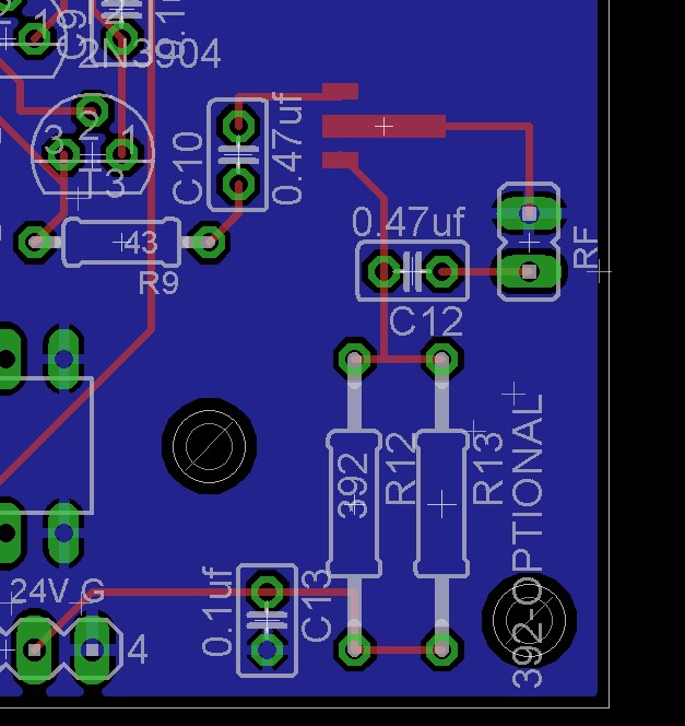
Here’s what my PCB current looks like:

I stamped a big orange “GALI” where the GALI-55 goes, in case there’s any confusion. It has three pads, two short ones for the input and output and one long one for the ground (the GALI grounds to this pad in two places). As we can see, there’s a thin trace running from the ground pad over to the header marked ‘RF’ where it connects to the ground plane. There’s another thin trace for VCC that runs from the lowermost pad of the GALI through the 0.47uF blocking cap and into a pair of bias resistors. I’ve only populated one of the bias resistors; the second was a ‘spare’ in case I wanted to use parallel resistors to dissipate heat.
So I take and I drill a hole immediately behind the GALI and ground it directly to the ground plane. Now we’ve got a good bulletproof ground.
Then I add a wire from the lowermost pad of the GALI to the bias resistor, R12. Now we’ve got a bulletproof VCC.
Nope, no luck, it still misbehaves.
The day I finally fix it…
Poking and prodding around the circuit the next day I find that if I move a grounded conductor next to the GALI, it’ll start producing gain again. Crappy distorted waveform, but it’s trying to work. So I drill another hole, run a conductor from the ground plane and stick the wire hovering over the GALI. It’s actually mostly working, but I’m not satisfied, I want to know more.
Then I have my first huge stroke of luck with this circuit. I accidentally touch a screwdriver to the unpopulated pad on R12. The one marked ‘bad’ in the following picture:

When I touch that unpopulated pad on R13, the output waveform changes drastically. However, when I touch R12, a mere 0.25″ further away, connected to the very same trace, there’s no misbehavior. A quarter inch of unterminated PCB trace is making all the difference in the world.
I take my screwdriver and scrape the trace between R12 and R13 right off the circuit board and the circuit is permanently fixed. I don’t even need my little ‘ground wire hovering over the GALI’ trick anymore.
So what do I think was happening? I think Robert was right about the high-frequency oscillation due to a layout issue. I think that 0.25″ trace between R12 and the unpopulated R13 pad was either acting as a tiny antenna, or providing some stray inductance or capacitance to the circuit. Just enough to throw that GALI into the high frequency oscillation state. Moving objects near the GALI, adding ground wires, etc., was affecting the behavior of that little trace. Even just a slightly different orientation of my scope probes was enough to have an effect, leading to the mysterious “it works!”, “it doesn’t work!” behavior when I disassembled the circuit.
Of all the projects I’ve done, this one has probably been the biggest learning experience. I’ve learned to have a great deal of respect for layout of RF circuits. I might even take the time to redesign and assemble a newer, better PCB.
The good news is, I probably didn’t ruin nearly as many GALI-55 as I thought I did. There’s three confirmed kills of the MMIC, but the rest of them might actually still be good!
I made a revision of the PCB to clean up the area around the GALI-55 — better grounding, shorter traces, room for an additional power supply filtering cap, etc. I’ll update this article when I get a chance to try out the new board.
Hi there
Just a few thoughts about your oscillating GALI amplifier:
1) The amplifier is designed to work at 50 ohms so all of those long thin PCB traces will not have helped. Proper 50 ohm lumped lines on the input and output would be better.
2) All of the GALI datasheets show a power supply line that has an RF choke in series but in your schematic it’s missing.
3) If all else fails and you still have an oscillating part try gluing a ferrite bead on top of the chip. It sounds crazy but it works.
Regards
Peter M Gant DL8OV
Darmstadt, Germany