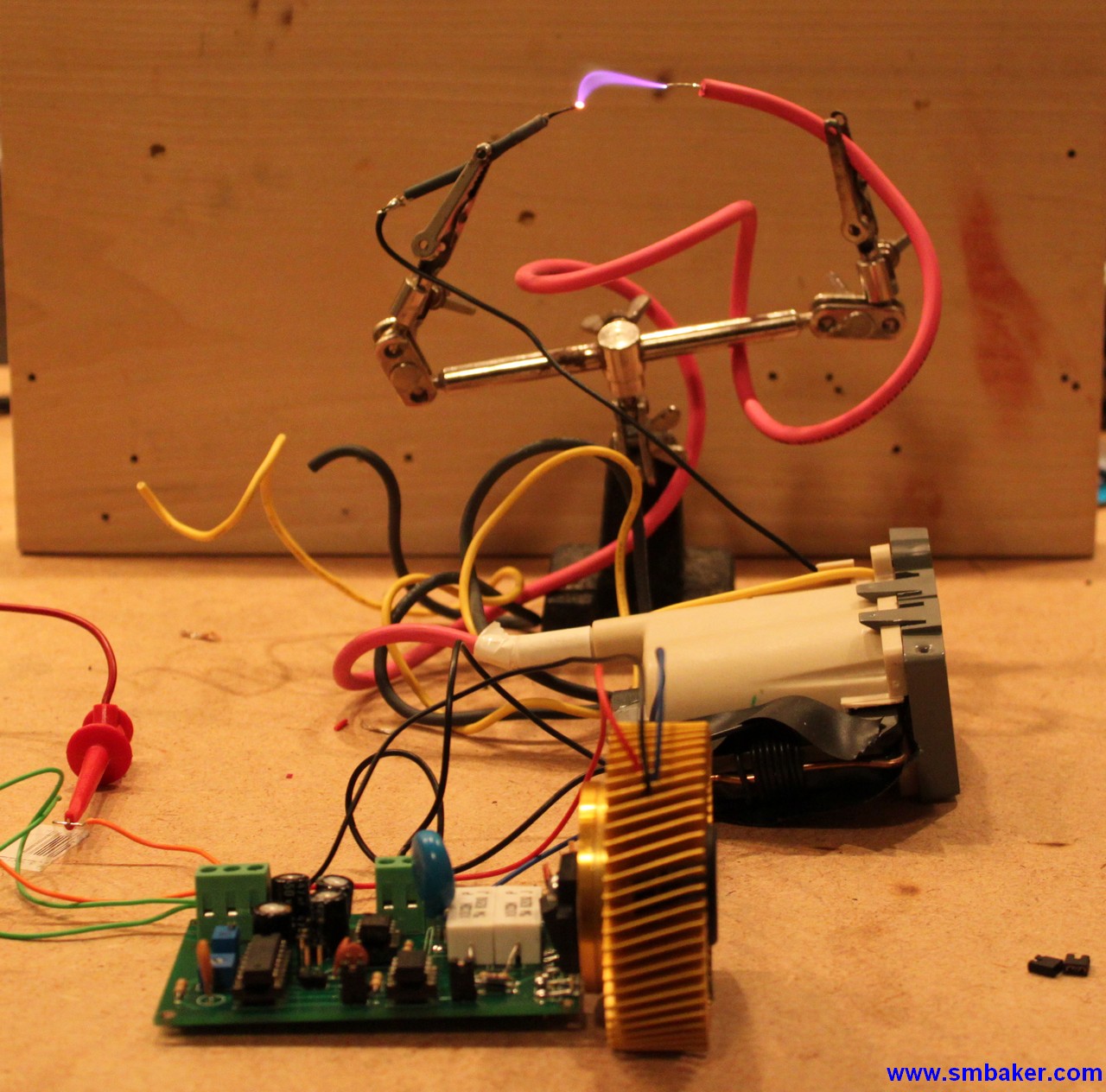
This project has been going on for years and has seen a number of prototypes, from a quick breadboard I made from an instructables article all the way to a custom circuit board. Here is a picture of the current prototype:
So what is a plasma speaker? A plasma speaker (aka “singing arc”) is a speaker that uses a plasma arc to produce sound. By varying the intensity of the arc, different pressure waves are created. Pressure waves produce sound. If you google plasma speakers, you’ll probably come across the instructables article — a lot of people have built that circuit, and this one is a variation of it. The problem is there is so much information in the comments of that instructables article that it’s hard to separate the fact from fiction. At one point I even went and built a “full-bridge” driver that I found there that I never could get working. Some more research led to the circuit that I have here.
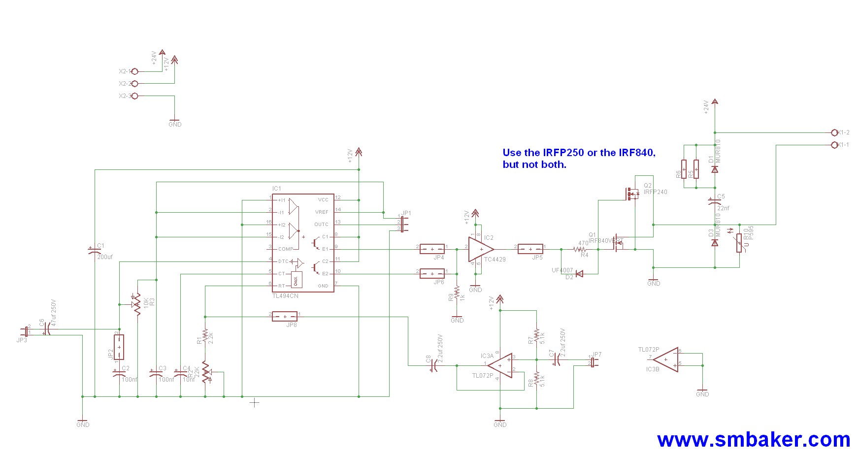
NOTE: Click on the schematic for the full-size version.
Let’s start with some of the basics.
Flyback. First of all, the flyback transformer. Most of these DIY plasma speakers use a television-style flyback. You can find these things on ebay relatively cheaply, or you can scavenge them from an old television. Flyback transformers are used to create the high voltages used to drive a CRT screen. High voltage is dangerous, so don’t mess with these transformers unless you know what you’re doing. Most people wind their own primary on the flyback. It’s pretty simple — you just wind 8-12 turns of wire around the iron frame.
Mosfet. We’re going to be dumping 5-10 amps of current into a very low resistance primary winding, and we’re going to be doing it at a fairly high frequency. To do this we use a transistor device called a mosfet. I’m not going to go into all the details of how they work, you can google that. The mosfet is the component that will be generating a lot of heat, and it’s going to need a heat sink. Without a heat sink, your mosfet can be ruined in a matter of seconds. The heatsink should have a fan. A leftover CPU heatsink is a good starting place. Commonly used mosfets are the IRF540, IRF840, and IRFP250. The board I made will accommodate any of these, although I chose the IRFP250 because it’s a monster in size compared to the others. By far the greatest problem with these circuits is blown mosfets from letting them get too hot and/or putting too much current through them.
Mosfet driver. One of the places where the instructables article went wrong is the lack of a mosfet driver and a pull-down resistor. Using a mosfet driver like the TC4429 (or MIC4429) is supposed to lead to cleaner turn-on/turn-off transitions on the mosfet, which is supposed to lead to cooler running and less potential for blown up mosfets.
Metal-oxide varistor (from Tobias’ blog). MOVs are used to bypass high voltage spikes to ground. I’m not entirely sure about how this is supposed to work because I had a lot of issues with it. Selecting too low of a MOV (35 volt or 110 volt) bypassed a lot of current through the MOV. This led to a nice cool-running mosfet but a very very hot MOV. I currently have a 450V MOV installed. It doesn’t get hot, but I don’t know if it’s doing anything either. I did blow a mosfet without it. The primary on the flyback will kick back an inductive spike when the mosfet switches off. I think the idea is we use the MOV to shunt that inductive spike to ground rather than letting it beat on our mosfet. More experimentation needed here.
Snubber (from Tobias’ blog). Ok, I’ll admit I don’t know a snubber from a hole in the wall. It was in tobias’ circuit, so I incorporated it into mine. I believe the goal here is also to smooth out some of the voltage spikes. I can’t tell if it’s doing much in my circuit or not.
TL494 chip. The TL494 is a pulse width modulator IC. It’s commonly used in switching power supplies. We’re going to use it to supply the frequency to drive the mosfet, which in turn drives the primary winding of the flyback. Some designs use a 555 timer IC. The TL494 seems to be overkill for the task. The TL494 has two different output control modes. There’s a parallel mode and a push-pull mode. We want the parallel mode, which in my circuit means jumpering OUTC in JP1 to ground.
Audio modulation (technique 1). So, our TL494 can supply a high-frequency drive signal to run our mosfet, which runs our primary winding. Now we need to modulate that frequency so that it produces variations in plasma arc, which will produce sound pressure waves. There’s two ways to do it. The first from the instructables article is to feed the audio into the deadtime control. This technique will change the width of the pulses that the TL494 is producing. By varying the pulse width we supply a different amount of energy to the primary winding, which will result in variations in plasma arc, resulting in our sound.
Audio modulation (technique 2). Tobias’ blog shows a different technique. He runs with a fixed dead time, but applies the sound via an op-amp to the RC section of the TL494. This will alter the frequency of the wave going into primary winding. By altering the frequence, we can produce different plasma arcs, creating different sound pressure, and producing our audio. I’m having a bit of trouble with this technique as it keeps throwing my mastech power supply into short-circuit protection mode. Have to work on it a bit, as I think it’s going to be the better technique.
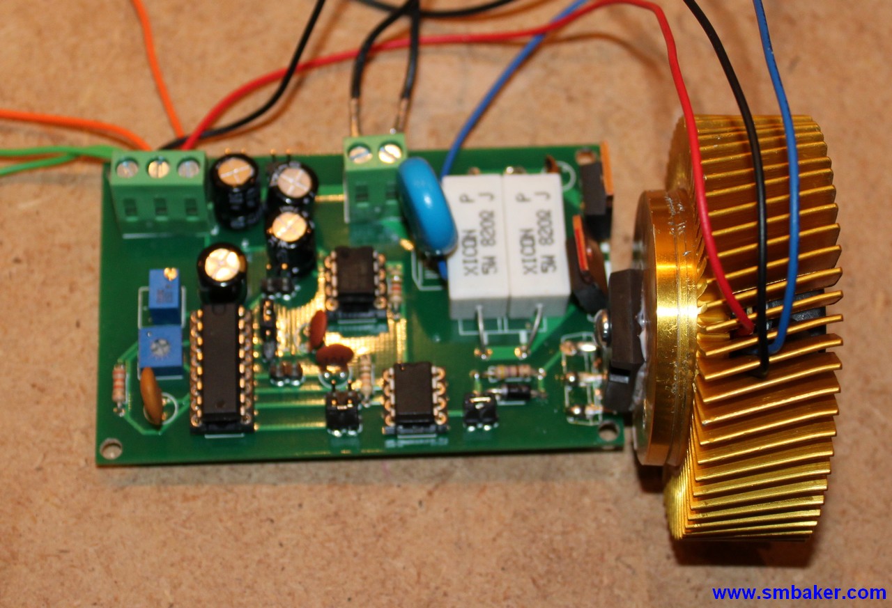
Now, some pictures of my completed board:
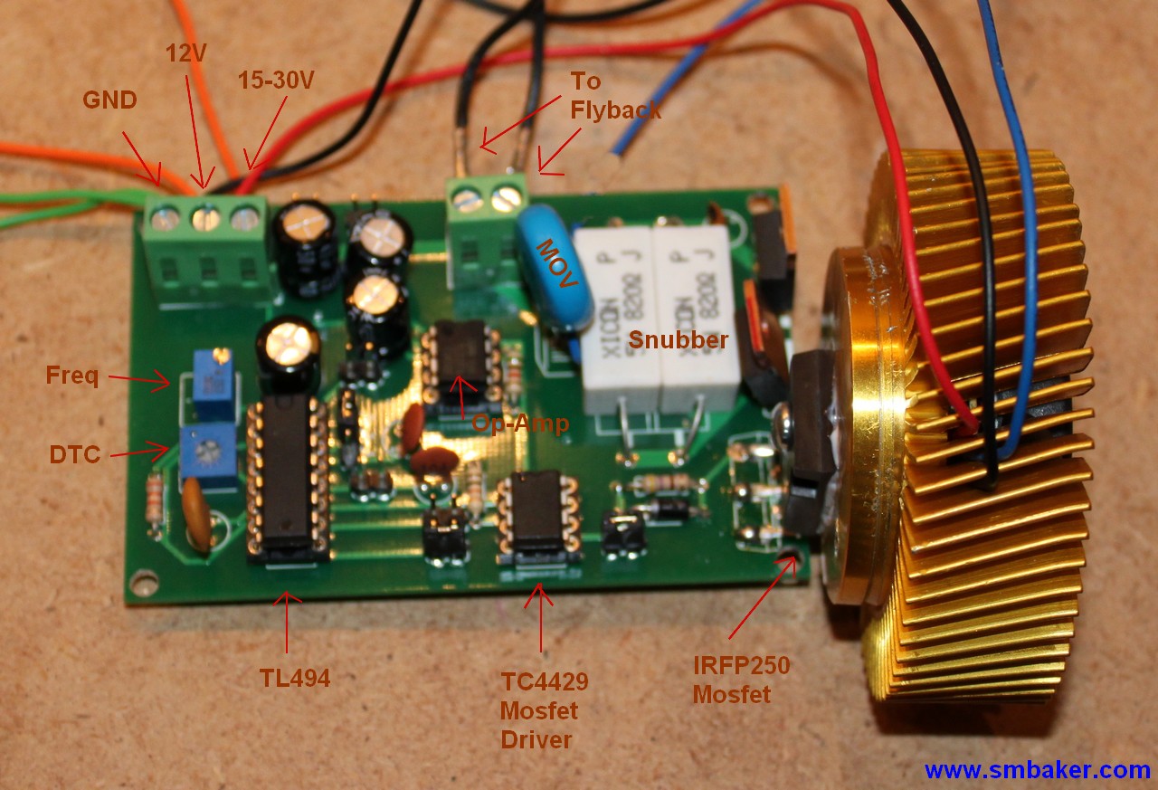
And, with some arrows showing the parts:
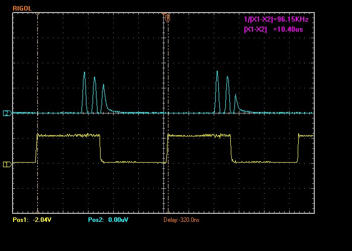
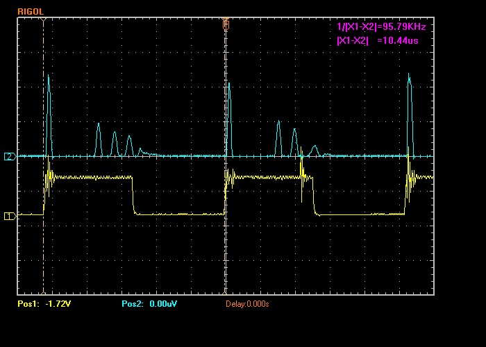
A couple of waveforms from the Rigol digital scope. Both waveforms are at 10V input to the flyback. The yellow trace is 10V/div and the blue trace is 10V/div. Yellow is the TL494 output to the mosfet driver. Blue is the wire feeding to the flyback primary (taken from one of the legs of the Mov). The first waveform is with the spark gap separated and no arc. The second is with the arc occurring. Frequency in both cases is about 96 Khz. No audio modulation in effect.
(click the waveforms to bring up full-size versions)
Ok, so the voltage on yellow is about 10.8 V peak-to-peak, which sounds about right for our TL494 driven at 12V. The voltage in the blue shows spikes in the range of 160V (pic w/o arc) and 230V (pic w/ arc). The TC4429 is an inverting driver, so when the yellow line goes high, the line to the mosfet goes low, and the mosfet turns off. I’m guessing the blue spikes are the inductive kickback from the primary, but someone with more electronic knowledge than me can confirm this.
Following Tobias’ suggestion, I added some capacitors in parallel with the flyback primary. Some experimentation is necessary here to find the correct capacitance. Adding capacitance may allow you to get a steadier arc at a higher frequency, so some back-and-forth tuning is necessary. I ended up using a pair of 0.01uf/1.6KV capacitors. My first attempts using caps rated at 250V led to quite hot capacitors; it could be because the inductive spike was in the neighborhood of 300V. 600V rated caps would probably be just about right.
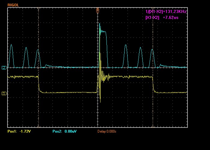
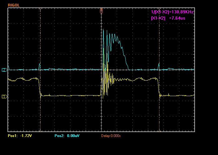
Below are some screenshots of the waveforms with arc, at 30VDC, 2 amps on the flyback primary. Frequency was upped to about 130 Khz. The one on the left has no caps, the one on the right has two 0.01uf/1.6KV caps in parallel with the primary:
(click the waveforms for a bigger view)
Adding the capacitors allowed me to get a higher frequency (130Khz) at 30 VDC and a lower current draw (2 amps instead of 4). The mosfet is now running much, much cooler than it did before, and I’m no longer running a hot MOV either. Sound is good, a definite improvement.
Version 2.0: The push-pull driver board:
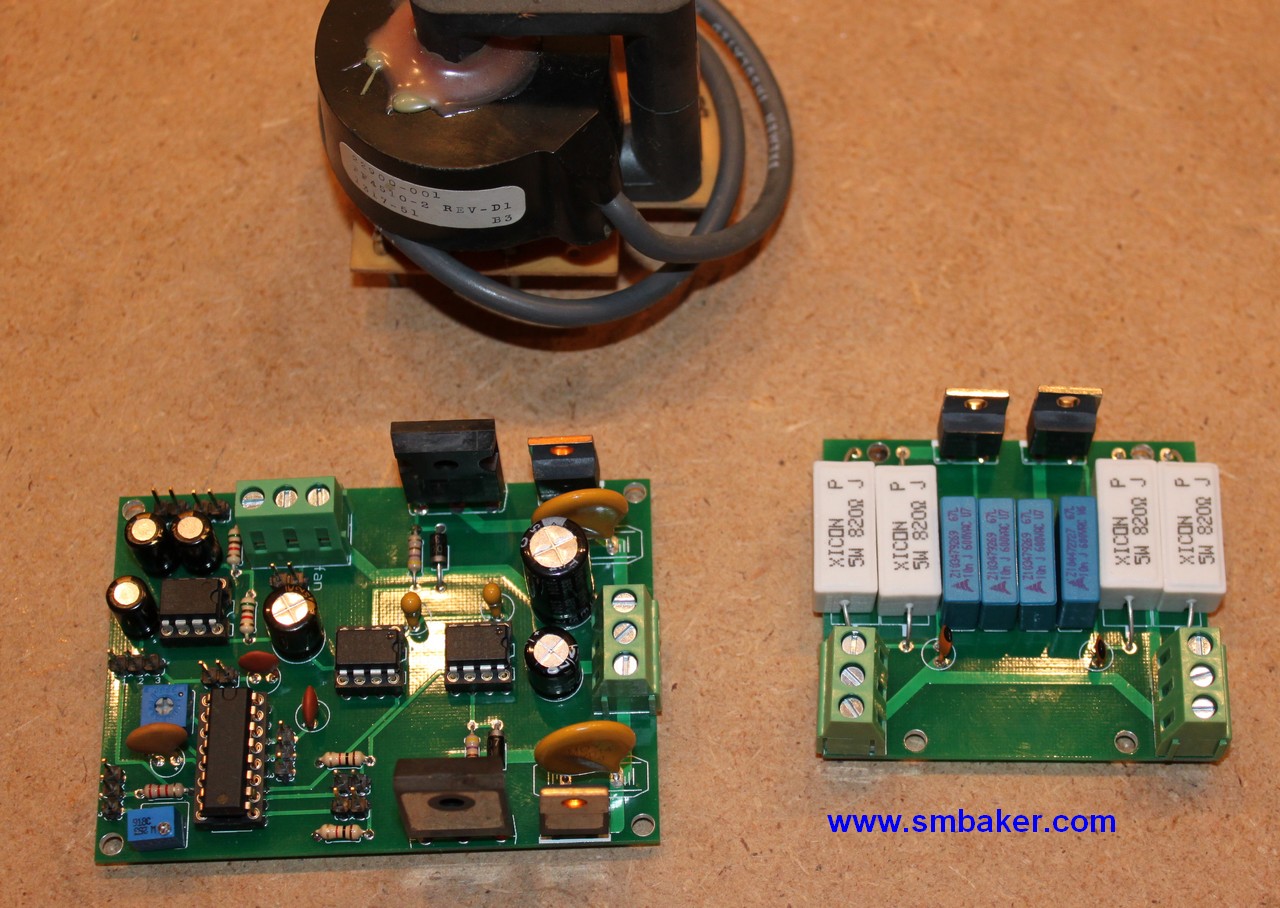
Started work on the push-pull driver board today (9/20/2010). Below is a picture of the newly completed push-pull driver board on the left, a separate snubber/capacitor board on the right, and an old-school flyback from ebay in the back. Taking the rest of the evening off to watch an episode of House (yes, you heard it here first, Dr. Gregory House, MD, is better than a plasma speaker) so trying out the circuit will have to wait a couple days.
Resumed work on the push-pull board today (6/26/2011). Has it really been nine months? I suppose it has. In that time I managed to completely rebuild a VW sandrail (see other blog posts) and build some cool dekatron gizmos, and actually get some real-world work done to earn a paycheck.
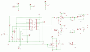
First, let’s have a look at the push-pull driver board schematic (it’ll be too small, so click for a much bigger view):
This board incorporates a lot of options. There are jumpers — JP4 and JP6 that allow each driver section to be jumpered independently (they should both be in place for push-pull operation). JP1 selects push-pull (1-2) or parallel (2-3). JP11 is for me to connect an external frequency pot (jump 2-3 to use the on-board pot). JP10 lets me use the op-amp for either frequency (1-2) or deadtime (2-3) modulation. JP7 is an input to the opamp. JP3 is for direct deadtime modulation, similar to the instructables article.
The snubber circuitry has been duplicated for two windings, and moved to a separate board.
The first thing I did was obliterate my new flyback transformer. I purchased some new transformers from ebay that were supposed to be some old-school ones that eliminated the diodes and extra windings and all the crap that the new transformers have. Unfortunately, I managed to quickly burn out the wiring on it, so I went back to the trusty old flyback from the original experiment.
So, a few things are evident with this board – 1) I don’t seem to be getting the frequency range that I used to. 2) I seem to have to run the deadtime pot maxxed out. I don’t remember the original board being that way; perhaps its a property of the push-pull circuit. I really should re-read the datasheet and remind myself how the TL494 worked.
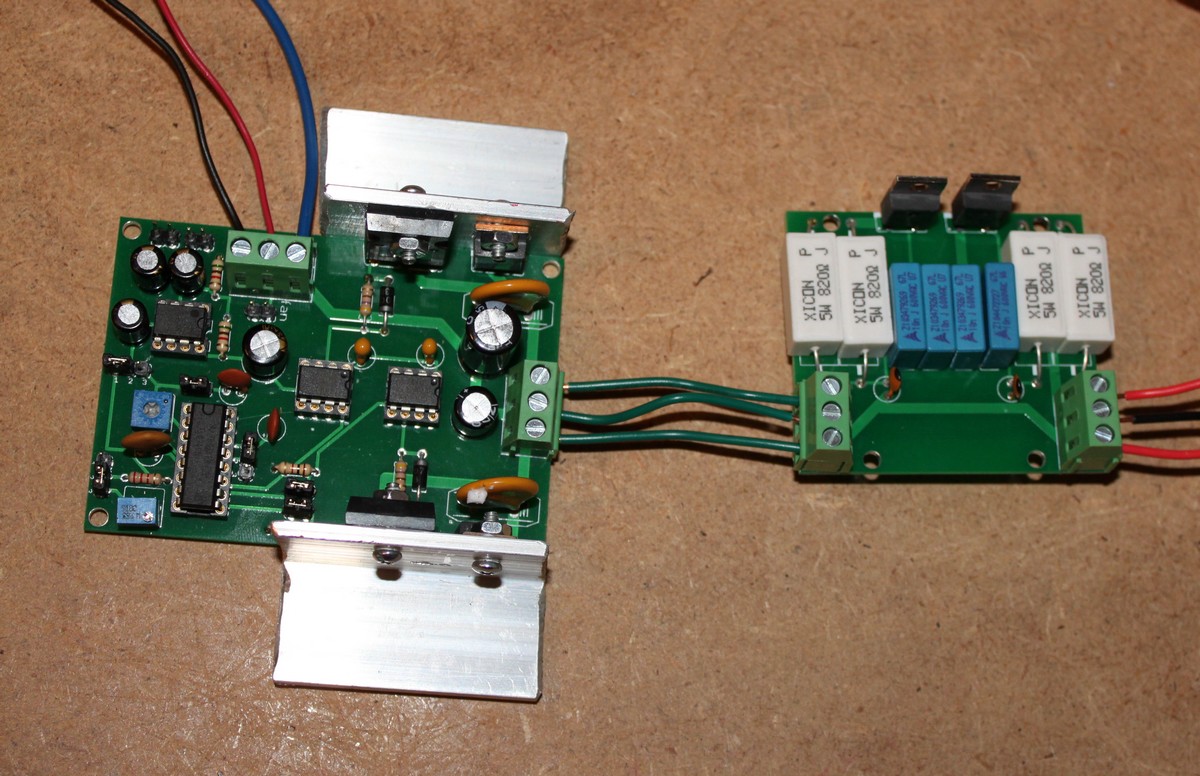
I’m also pulling more power than before. To get a good sounding arc (and it does sound good), I’m pulling 6-7 amps at around 12-14 VDC. I can’t even drive the circuit beyond 17 VDC, because I’m quickly maxxing out the current capacity of my power supply. Being a little careful because I don’t want to burn out more mosfets (so far, so good). I’m sinking the mosfets with just a couple pieces of aluminum angle iron. Here’s a quick view of the experimental setup:
So, anyway, things to figure out for next time — why is this pulling so dang much current? perhaps I should use longer windings on the primary? I’m also going to have to remind myself whether I was frequency modulating, deadtime modulating, or something else on the old board.
References. There’s a lot of research that I did (getting this thing to work has been over 2 years work!). The two primary references I used are:
- The instructables article: http://www.instructables.com/id/Build-A-Plasma-Speaker/
- Tobias’ Blog: http://tobiasmugge.wordpress.com/projetos/plasma-speaker/
Finally, a youtube video of my plasma speaker, as it currently functions:
Scott
Very good work you did here! The IRF250 you got is way better then my already very expensive in Brazil 540. And very clean PCB. Mine home-made board blew some traces so…
About the MOV: I think you really don’t need them if the system is well tunned. The problem is that while you are tuning it the FETs blown one after another… If it is tunned a 110 V MOV should not heat too much. Same to the snubber resistors. Mine smoke several times.. but at least the mosfet was happy.
Do you have a oscilloscope available to tune your system? It helps a lot with frequency modulation!
Good to know that I on google! hehe
Best regards and good luck with your project
Tobias
Thanks very much for all the comments, Tobias. I found your site very helpful in my research. The snubber resistors aren’t getting hot yet, but I do have two 5-watt resistors in parallel, so that’s probably giving some pretty power handling capacity.
I too have blown many mosfets while working on this project. Most of them were IRF840s or IRF540s. That’s why I decided to try out the IRFP250. The current board I created is actually setup so that either mosfet can be soldered in place.
I do have an oscilloscope available, but I’ve not yet figured out the procedure for frequency tuning. Any tips you can provide would be helpful.
This picture shows the voltage on the primary while I was tuning the system:
http://tobiasmugge.files.wordpress.com/2009/03/p250509_09-55.jpg
That’s the best I’ve got but can be tuned better.
Are you using a cap in parallel with the primary on the flyback?
It’s difficult to choose the value because you have this capacitance, the number of turns on the primary, the frequency and the dead-time to adjust.
Fix the dead-time around 40% and start from there. Change capacitance, search for the best frequency. The right one is when the arc is not that hot but consistent and the current consumption is low. You want to work something between 60 and 100 kHz. More frequency equal better sound.
If the freq is too high or to low just change capacitance or turns. But stay around 12 turns for 30 V. And start tuning with a low voltage, like 12 V.
To fine-tune change the freq and dead-time until the wave of the voltage on primary reaches the ‘smoothest’ point.
Yes, it takes a loot of time!
Hello Tobias, I don’t have a capacitor in parallel yet. Are you just doing that for tuning, or for general operation as well?
I haven’t got the scope out yet, but I was playing with the circuit tonight and tuned it to what sounded best. I’m now getting somewhere around 4 amps at 30 volts. I still ended up burning out the mosfet after a while of continuous operation (I’m thinking the CPU fan I have is not adequate enough for extended operation).
There’s something a little weird with starting the arc at my current tuning. To “start” the arc, I have to close the gap down to about 3/4″. Once it’s started arcing, I can easily open it to 2-2.5 inches or more.
Got the oscilloscope out and made some measurements…. they’ve been added to the post. Not entirely sure what I’m looking for at this point. I haven’t added a cap to the primary yet.
I used Richie’s site as one of my references. From there Ive got the snubber design. You want to reach the Vc waveform:
http://www.richieburnett.co.uk/temp/flyback.gif
Mine is pretty close as you can see on the picture of my site.
That waveform gives me a 1″ starting arc. I did not tried to stretch it up.
With 30 V, only ~2A. Depending on the modulation, 2.6A. And no burning fets.
The cap stays there for operation!
Best luck
Very interesting results. I started playing with capacitors. The first few I tried (2.2uf and 1uf respectively) increased the amperage significantly. However, when I got to the lower values in the parts bin, that’s where things got interesting. An 0.047uf/250V cap reduced the current draw by about an amp, but the little cap started to get quite hot. I started playing with some 0.01uf/1.6KV caps and found that with two of them in parallel I was able to increase the frequency to about 120Khz, dropping the current draw to about 2 amps. Four of them in parallel drops the current to around 1.6A, but I’m tapped out as far as I can go on the pots for lowering the frequency.
I finally have a COOL running plasma speaker that sounds pretty good. As far as I can tell no more fried mosfets or hot MOVs.
Time to start work on revision 2.1 of the driver board…
Very good results!
Good to know that you did it.
Are you in USA? It’s quite easy to you to buy FKP caps out there.. Those does not get hot.
Maybe we can help each other designing this rev2 board? Tell me how many bucks it costs to make a industrial board there.. Here in brazil it’s like $60.. a little fortune! hehehe
A tip: the PWM signal circuit cant be close to the power section of the board. Take a look on yours. It’s pretty close. This lead to noise…
Yes, I’m in the US. Some of the capacitors I have laying around are Wima caps (from Mouser, I think). I’m not sure about these particular 0.01uf/1600v ones though. I’ll have to double-check where they came from.
Generally I get the pc-board from batchpcb. The cost to make the last board was only about $17, but one has to add $15 shipping and handling to that. I usually batch up several different projects together so I can save on the shipping and handling fees, so it’ll probably be a while before I submit the next plasma revision. The new design is already slightly bigger, and batchpcb charges by the square inch, so it’ll cost a bit more. I have moved some parts around a little bit. In particular, the op-amp is no longer next to the high power section and has been moved to the other side of the TL494 where the rest of the low power stuff is. I’ll see if I can post an image of the revision when I get a chance.
I’m thinking of modifying the design to a push-pull design (or at least have the option of doing it). I don’t think this would be hard to do — it’s basically duplicating everything on pin #10 of the TL494, sticking it on pin #9, and switching the output control jumper. Then we put a center-tapped coil on the flyback. I’m assuming I would duplicate the snubber as well. This could all end up a much larger board which is a little unfortunate. I might try some experiments first to see how much better the push-pull design works.
In my next plasma speaker project I would like to get rid of that 4429 IC to try a GDT.
494 -> BC transistor -> GDT -> FET
And go for bigger FETs as you did.
The problem is that here in Brazil anything unusual is too hard or to expensive to get. Or even both. The 4429 is both.
Are you trying to do a halfbridge design?
No, I’m going to try experimenting with a push-pull design… If I understand correctly, this is different that a half-bridge. Whereas the half-bridge is switching a single primary between +V and -V, a push-pull uses a center tapped coil, with +V at the center and alternately switches either end to -V. The design was suggested to me in one of the comments to my youtube video, so I’m going to give it a shot. Of course, my knowledge of switching supplies is very limited, so I may not be understanding correctly. 🙂
Anyhow, I sat down to look at my schematics tonight, and before I knew what happened, I had a design ready and sent off to batchpcb. Should have the new board in a couple of weeks (batchpcb is rather slow). It’s easy to get carried away when one sits down with the schematic software…
As far as the TC4429s, I got them from digikey at about $1.72 each. Seems like I shopped around to get a good price on them, but unfortunately I only grabbed a limited quantity (didn’t know at the time my summer free time was going to be dominated by plasma speaker projects!).
I thought I would write you and tell you how much I appreciate you sharing you experience and your design. Few people on the internet have shared a complete Schematic. I look forward to seeing a video of you new push pull design.
I hope I can purchase a PCB from you when you are satisfied with your design.
From your comments to Tobias your explanation of how the a push pull works sounds correct to me. I would very much like to follow along with you during your design adventure. I am no expert but I am well read and I have resources that may be helpful along the way.
Feel Free To E-Mail me
Good Luck.
Could you explain you preference of FM over PWM, please?
Thanks for the comments, Peter, and thanks for setting me in the direction of the push-pull design. I’m looking forward to seeing how it compares to the current design. We should know in about 2.5 weeks! 🙂
As far as the Pc-boards, I use batchpcb, and they have a marketplace. I’ve held off on listing them publicly so far until the design(s) are finalized, but once they’re ready I’ll definitely list them so that people can order a board. Processing from batchpcb takes a little while, but getting a quality double-sided silkscreened and solder-masked board is worth the wait.
As far as FM vs PWM, I thought the FM sounded better. The board is designed to support either method (in fact, you can even use both at the same time; it would be interesting to feed two different audio sources and see what happens). The latest revision will have the option of jumpering the op-amp to either. As far as why the op-amp is there, it came from tobias’ design…
Thanks again for the comments!
You need that op-amp to have a high impedance audio in. It works together with the capacitor that follows. This last one changes the reference from 0 V to 6 V to source the TL494. Connecting a capacitor this way ensures that no DC voltage differential will be created between the op-amp and the tl494. Only pulses pass throw the cap.
When you read on the net that people blew some audio players off experimenting with plasma speakers that’s because they did not use a high impedance audio in =)
The finest plasma speaker circuit I’ve ever seen. If possible, can you please also publish your PCB design?
I was planning on holding off putting the PCB pattern up (and the link to manufactured boards at batchpcb) until the next revision is done as there are a few important changes I made. I definitely will do so when the new boards arrive, thanks for the comment!
Thank you, I’m looking forward to it. My biggest problem is FETs’ heat dissipation; I’m thinking about how to absolutely avoid linear mode, maybe with an additional switching-mode FET driver. This is only a plan, I haven’t tried that yet.
I can’t wait to see your new board. The suspense is killing me. I would really like to know what you thoughts are on the Push Pull system. I already started ordering the parts for your board when you make it publicly available. May be a quick up date would be nice. Thanks and keep up the good work!
great info! very impressive work!
I and every one else following you would appreciate an up date on how the new push pull boards are going. Thanks. 🙂
Any updates to the schematic? I have been looking over the parts, and getting setup to make one for myself. I have also been wondering if the input audio can raise and lower the volume of the “speaker”?
Can’t wait to see the next revision! Out of all the system’s I’ve looked at this seems one of the best designed
How is it going. Are you blasting some matalica on your new plasma speaker yet. LOL . An up date on you web site once in a while would be nice. Thanks and keep up the good work.
Peter
Do you think a 163 volt clamp 80 volt DC rated MOV will work. I am building my own prototype and need advice on picking a MOV. Any Advice would be help full. Thanks.
Hello ther thank you for your post, i have been searching for plasma speaker and i did like very much yours, i wounder if you mind to send me the list of materials necessarie to do the entire build. Thank you so much
Ty for the prints, i was searching for a good FM build and these fit the bill brilliantly. http://hv-labs.xf.cz/images/singarc/budic-mustek.png
I plan on implementing push pull like this soon.
You did a great job, and just like you , I have been working on plasma speakers for 2-3 years now (ever since I started College). I have been looking at Tobias’ design for quite some time and have found it to be one of the best designs as far as run time goes. But my plasma speakers generaly fail miserably for unknown reasons like my lastest one. One day I test it and it worked beautifully, nice arc with clear sound and no heating of the mosfet or other components. It was like a dream come true from my other designs which blew mosfets like firecrackers. Well a week later after it ran just fine it decided not to work anymore – didn’t touch it- it just didn’t work anymore. It tries to draw over 5amps from the supply and then I thought I wonder if its like what u were saying about the 1st technique in audio modulating the flyback by injecting the audio into the RC timing section and not the dead-time. I really just think my plasma speakers have a grudge on me or something… Other than that every component is fine and functioning normally – leaves me stumped and stupefied. Have you come across this problem were it would just not work anymore for no reason? I can tell you another interesting thing is that my low power side has a separate ground then my high power side and when connecting them both together I get a really week arc and the mosfet gets hot quick, another wierd thing.
Any luck with the new design?
Thanks for sharing the high voltage PSU design!
I haven’t had a chance to try it out yet… work has been keeping me busy 🙁
Do you plan on continuing your testing and design of your plasma speaker in the near future?
I am interested to hear about the new design! Been waiting for months. I like your wordpress template too ; )
Yes, I’ve had some more free time lately, so I think I might be able to get some more plasma speaker work done!
Still wondering how the Plasma Speaker Project is goning?
Thank you for the update. Were you able get a longer ark with the push pull than with the half wave? May be you could put up a quick up date video. I would Really appreciate it. I had a printed circuit board made based on Tobias and your design. It includes the Push pull also. I will let you know how it goes when I get it up and running. Best wishes.
very nice project! i’ve also found the instructables website already and was planning to build one as well. I guess you took a decision with the higher voltage varistor, they seem suitable only for limited pulse loads: http://www.resistorguide.com/varistor/
This is a very nice project, and has my interest piqued, but there are some aspects that are just painful to watch… If I may…
1, why are you using MOSFET driver chips for this? My gut instinct without looking up the FETs you’re using is that the Vgs requirement is excessive. There are several MOSFETs that are better suited for the switching here, and have a much lower Vgs rating. IRFZ44N for example – can be saturated at around 6V. They also have a much better current handling ability, and if for added insurance against popped transistors, get one that is avalanche rated. I drive flybacks experimentally all the time with no snubber whatsoever, no problem. I include them in printed versions of my projects for added insurance, but a suitable transistor can handle what a flyback can dish up. The 494 has a more than adequately qualified totem pole output that can drive these transistors directly.
2, Snubbing reduces the effectiveness of a flyback transformers operation. You WANT rapid collapse of the field in the core to get maximum output efficiency. Snubbing steals some of this energy away from the system, reducing the output, requiring more drive.
3, Try going more with very low duty cycle to establish your arc. This can be difficult to do, as you’ve discovered. Using the caps in parallel with the primary can help, but just as with the snubbers, this method can reduce efficiency. The mechanism is different however, involving dv/dt rather than raw “theft” of the energy. Low duty cycles will help with this, as it will operate more as a class C system than the brute force method that is evident in the scope traces. Less is more in this case.
Last but not least, PWM is your friend here. Tune the chip to the transformer and let resonance do the work! More duty cycle means more current in the arc, which means more heat, which means more air displacement. Let the transformer do the work, not your power supply and MOSFET. You’ll be able to get more SPL out of it, and the transistor will run much cooler.
Email me if you have any questions.
Steve
Great site.
I just built a similar plasma speaker using the same TL494 chip and a MOSFET driver. Works great apart the FET gets very hot even with a big heat sink. Can someone explain why the output of the MOSFET driver is via a 470R and not directly connected to the MOSFET. Would the MOSFET switch quicker if connected directly to the driver chip?
This is a very interesting project, I would like to build one as well. I’m not expert with electronics stuff but I think I can manage it easily, (high voltage, soldering etc not an issue). I have some difficulties to understand the schematic for the version 1.0 of your board. I kindly ask you if you can help me also P.M. with a “foolproof” schematics of the complete board. I would Really appreciate it. Best wishes.