The Zilog Z8000 CPU board is the brains of the Z8000 modular computer. Remember, you can always go back and read the Blog Post or watch the videos to learn more.
Click here to return to the Z8000 master board index.
The CPU Board contains all of the following:
- Zilog Z8001 Microprocessor
- Memory addressing and Bus decoding logic. The Z8000 has 8 segment bits and several different states (data read/write, program read/write, system vs normal mode, etc) that makes memory addressing a little bit complicated.
- IO address decoding for four common peripherals — SIO, CIO, and CompactFlash. Putting these on the CPU board allows reduced chip count on the other boards.
- Address latching / buffering. The Z8000 is one of those CPUs that multiplexes address and data on the same set of pins.
- Data buffering. The data bus is buffered for both reads and writes to reduce drive requirements on the CPU.
- Reset logic. When the system is reset, it loads the initialization vector from the Flash ROM image, then it reconfigures itself for regular memory access.
The schematic of the Z8000 CPU Board is shown below:
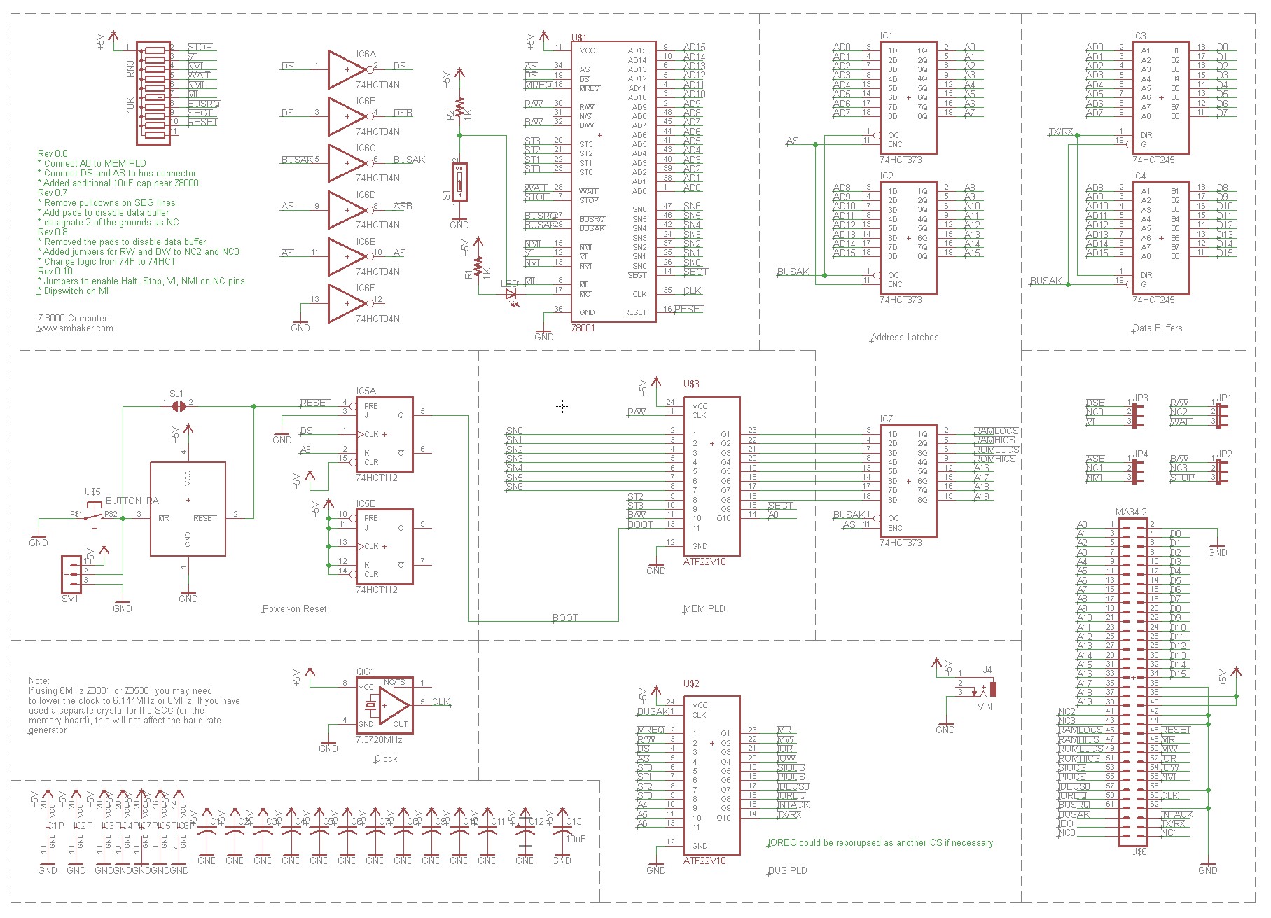
Click the schematic to get a bigger view, or go into the github link at the bottom of the page to find a PDF of the schematic.
Bill of Materials (BOM)
I always have lofty ambitions about filling out the BOM section…
Building the CPU Board
First you have to choose whether to build the 4-layer version or the 2-layer version. My personal preference is to go with the 4-layer board. It’ll cost a couple dollars more, and a couple days fabrication time longer at the board house, but it has much better power distribution.
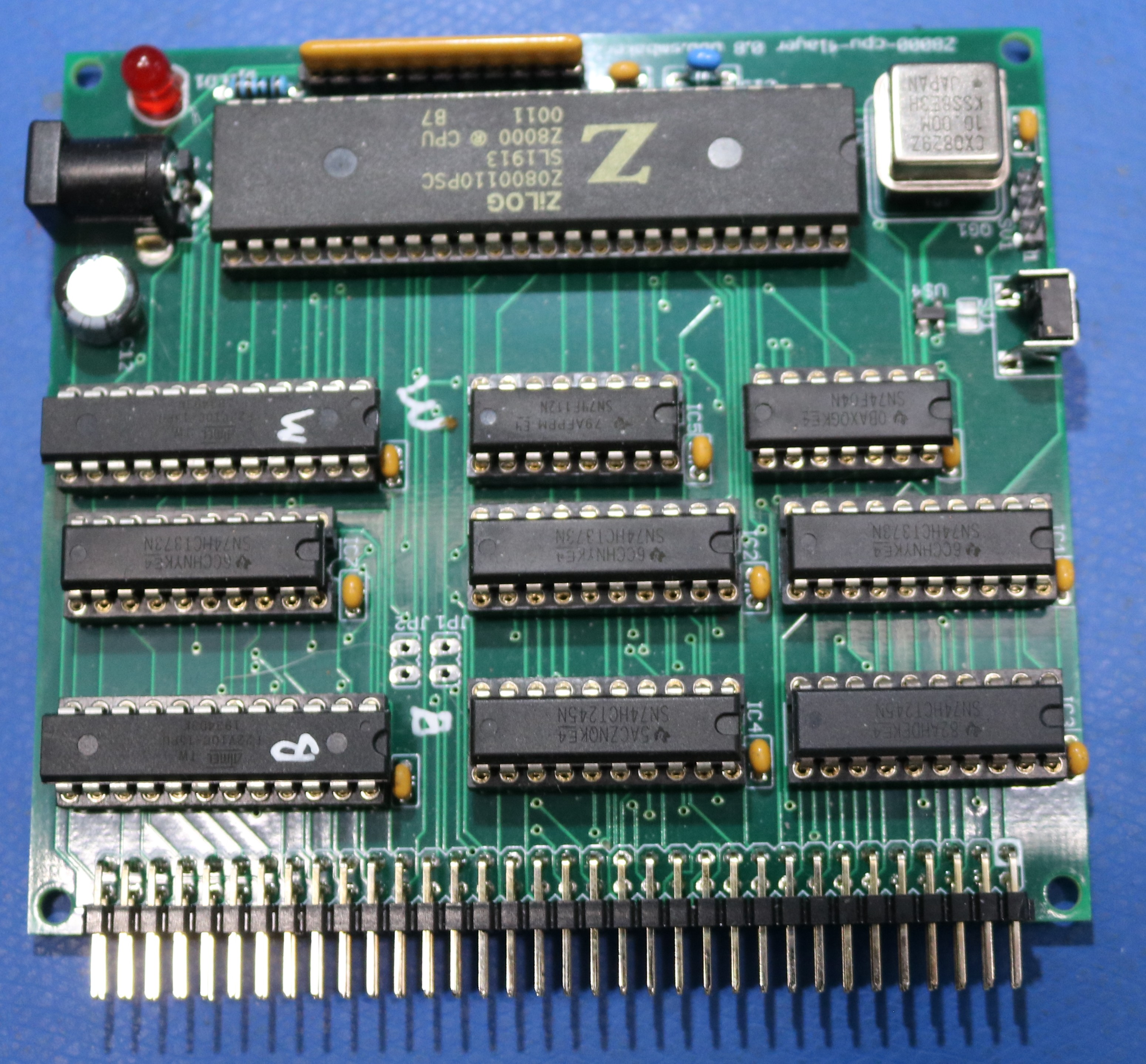
Board Images
Gerbers
- Github link to PLDs (you want both the bus and mem PLDs)
- Github link to Gerber Files