In this post, I build a single-board computer that uses the world’s first commercially available CPU, the Intel 4004.
Background
I’ve previously done projects using the 8008, the world’s first commercially available 8-bit microprocessor, and I’ve always wanted to do some projects using the 4004, the first commercially available microprocessor (dropping the “8-bit” qualifier; the 4004 is 4-bit). I’m saying commercially available, because as one reader points out, there was a classified navigation computer for the F-14 fighter airplane that preceded the 4004.
I started the project by visiting Jim Loos’s page, as I did with the 8008. Jim has a great little project with a simple easy to follow schematic that breaks down the various subsystems (CPU, RAM, ROM, Peripheral Controller, etc). From this, it was relatively easy for me to design my own board, keeping the core building blocks the same.
Design
The full schematic as well as the gerbers you can find in my github repo. Here I will present a few select pages from schematics that I think are worthy of discussion.
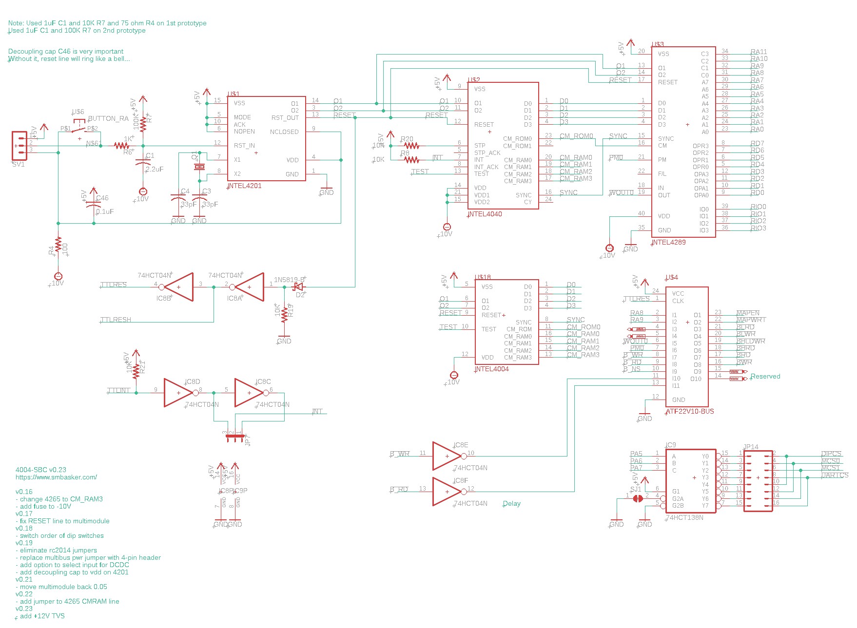
The first page has the 4004 (or 4040) CPU. For the purposes of this project, the two CPUs are essentially interchangeable, and my SBC implements both sockets. To the left of the CPU is the 4201a clock/reset generator and its crystal. To the right of the CPU is the 4289 Standard Memory Interface. You’ll notice that the 4004 has a 4-bit bus, together with some sync and select lines and a clock. Ordinarily it would require special rare ROMs that worked with that bus. The 4289 does the magic of converting that 4-bit interface into something that resembles an 8-bit ROM interface, so we can use plain ordinary ROMs. The 4289 also offers an IO port, which is pretty handy.
Also on page 1 is a PLD that I used as a dumping ground for miscellaneous logic, and a 74HCT138 that I used as a chip-select for some of my on-board peripherals. I used a couple of inverters to condition the RESET pulse into something that I can use with TTL devices. Note that the 4004 uses 15V logic, with +5V VSS and a -10V VDD. Not the most convenient logic levels to interface into more modern TTL or CMOS devices. Next up is the power supply.
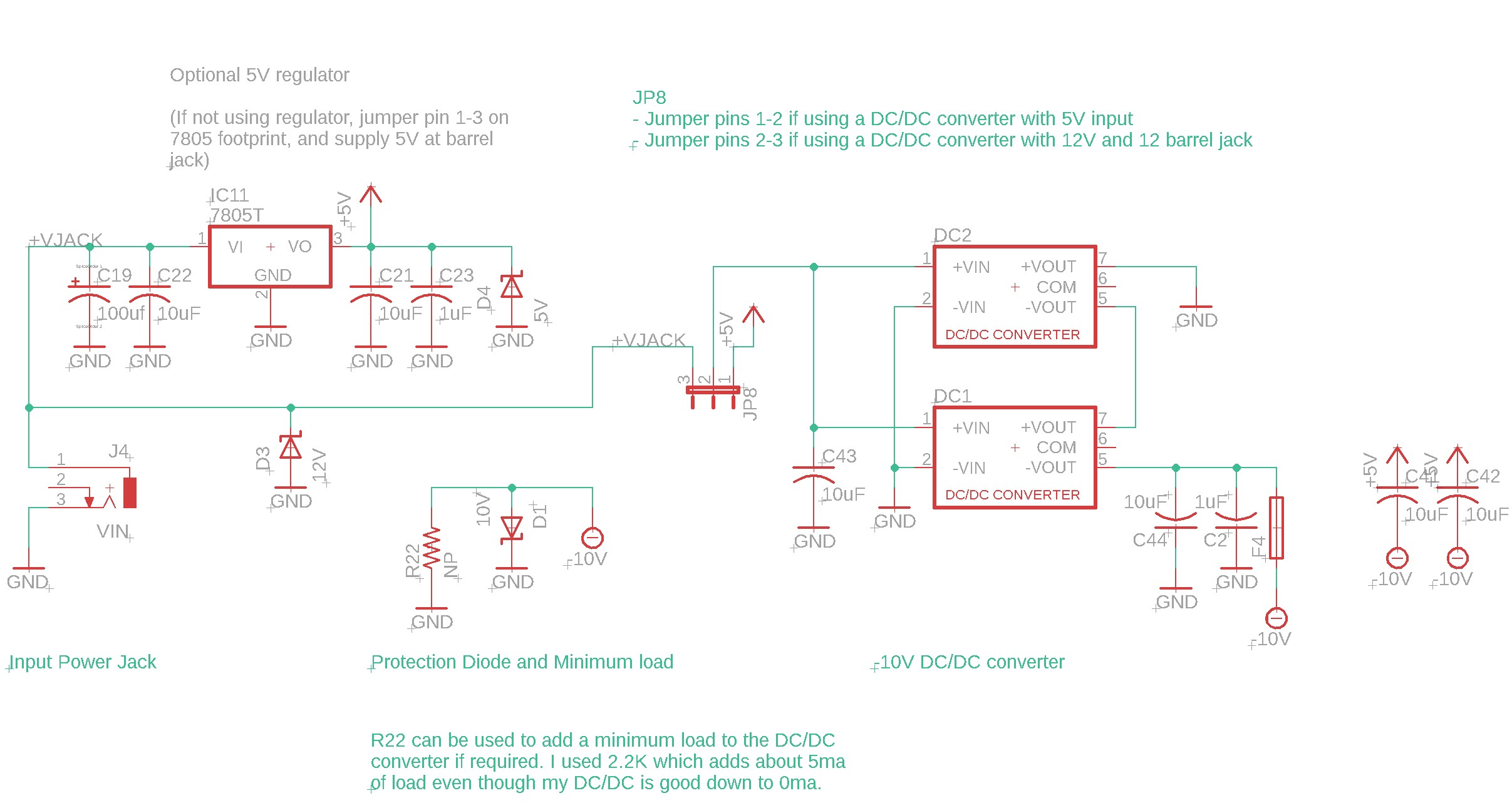
As I mentedion, we need +5 and -10V. I got the -10V by using a pair of isolated 2W DC/DC converters. Each of these DC/DC converfers produces 5V at 400ma. By putting them in series, you get 10V at 400ma. You can choose DC/DC converters with different inputs — I have experimented with ones that use 5V input and ones that use 12V input. In my experience,. the 12V-to-5V converters were cheaper than the 5V-to-5V converters. Set the jumper (I recommend you solder it permanently) depending on which type of converter you choose.
For the +5V supply, you have two choices. If you used 5V-to-5V converters, then you can simply jumper across the 7805 footprint. If you used a +12V footprint, then you’ll need to populate the 7805. Rather than a real 7805, I chose an ezsbc 5v switching regulator that fits the same footprint. It provides up to 3A of power. Next up
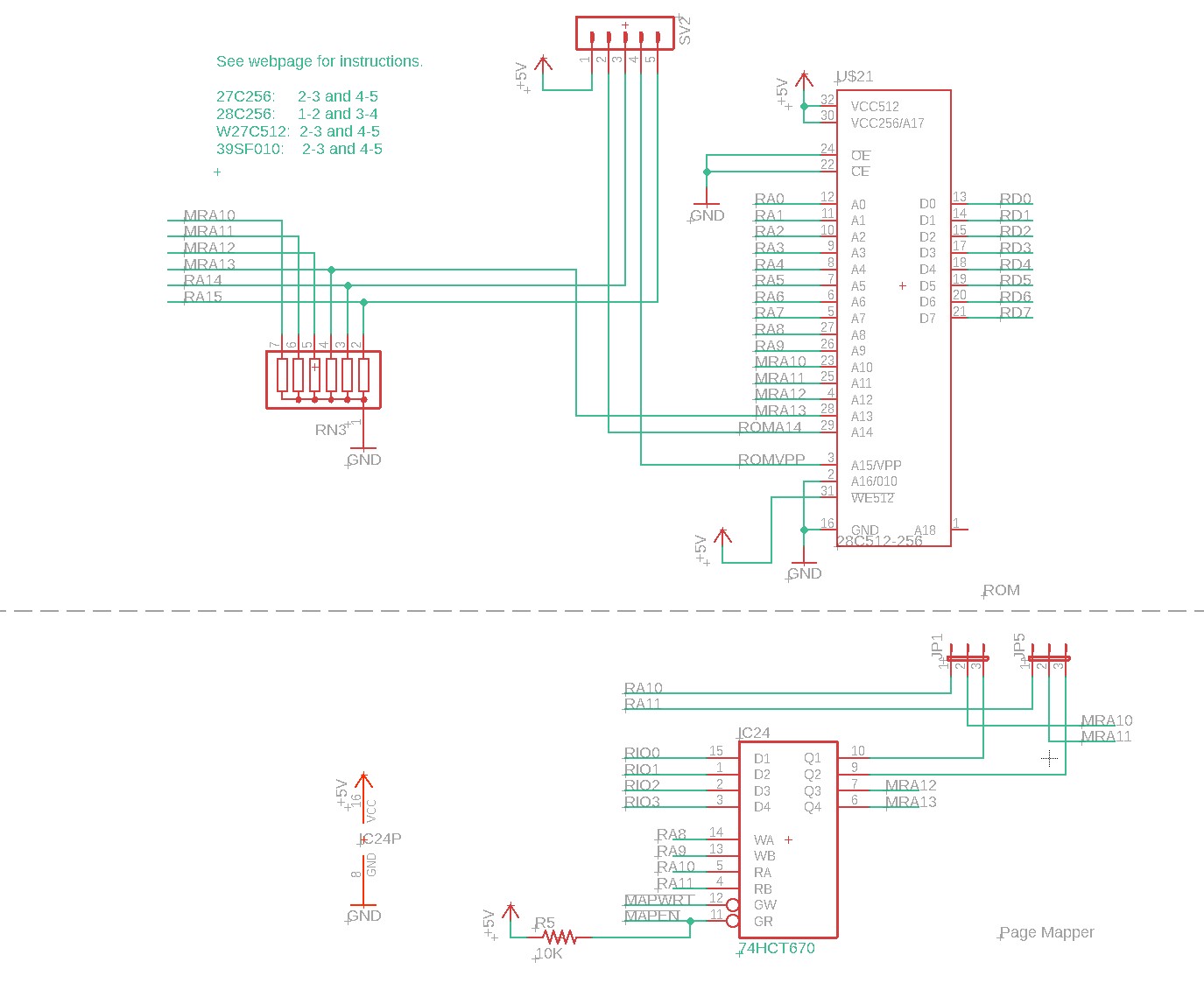
Here we have a socket for the ROM, which is connected to the 4289 back on the first page of the schematics. I also added a 74HCT670 register file to serve as a “page mapper”. The 4004 natively supports 4KB of ROM. Using the register file, I can page this, in 1KB page sizes, across a 16KB ROM space. This allows me to have four complete banks (i.e. 4 sets of 4KB) to have more programs available. Next up is the serial interface.
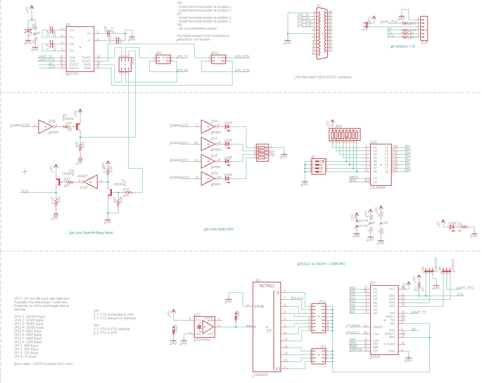
There are actually two serial interfaces here, of which you have to select one. First, I copied the “bit-bang” interface from Jim’s project. Bit-bang requires the CPU to do all the timing. The CPU is busy doing this whenever it needs to communicate, and your baud rate depends on your master clock. The other option is an 8251 UART and a MAX202 driver. These are more modern / less vintage, but frees up the CPU and gives you the option of a plethora of baud rates. A pair of jumpers selects which one. Also here are some LEDs connected to the IO port on one of the RAM chips (you’ll find the RAM chips on a subsequent page) as well as a set of dip switches. Next up is an RC2014 bus.
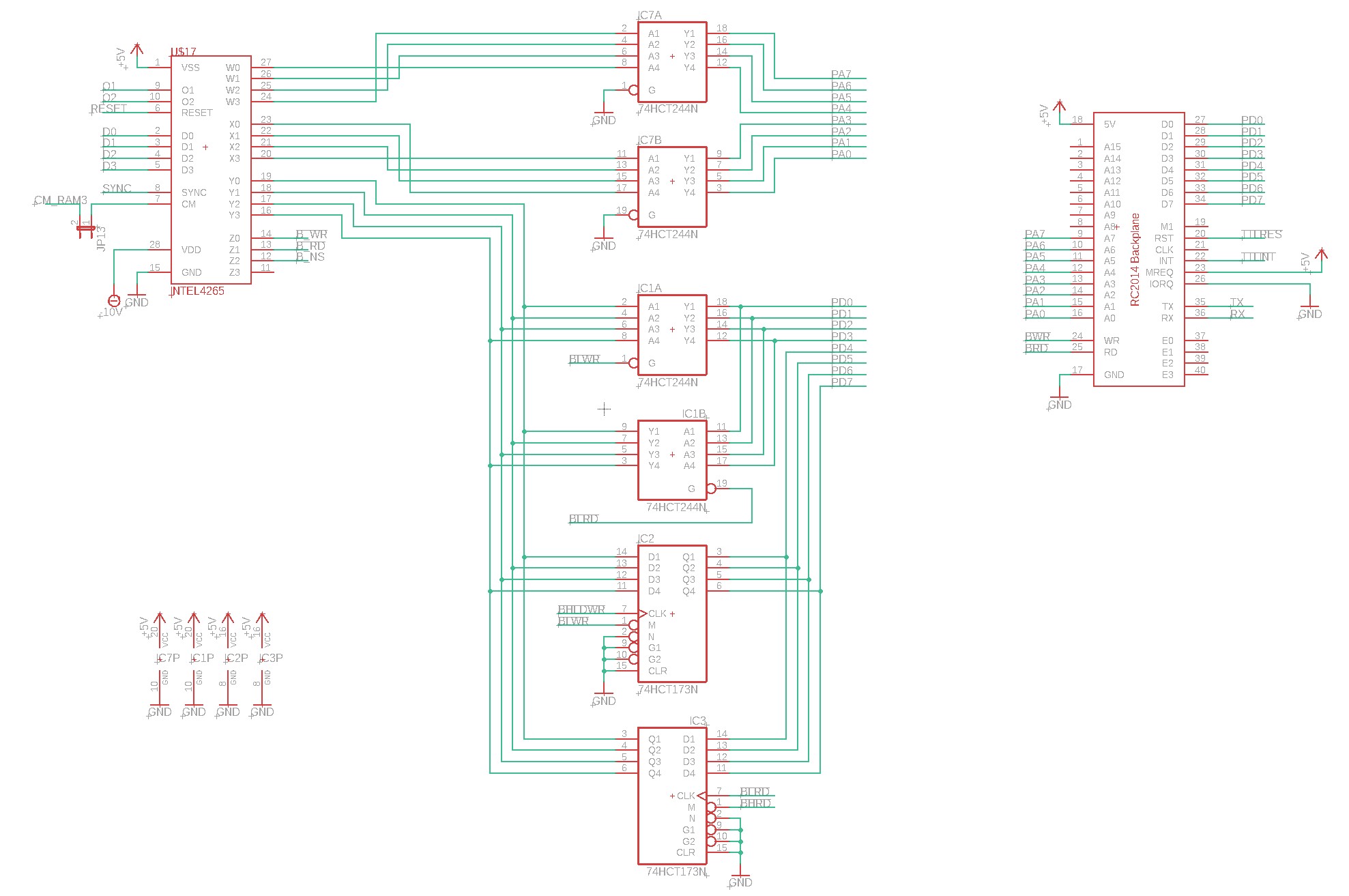
The RC2014 is an 8-bit bus, and we have a 4-bit CPU. How are we going to manage that? Well we’ll use a 4265 peripheral interface IC. It takes the 4004’s 4-bit bus and turns it into four 4-bit IO ports. There are a number of modes supported. We’ll use mode #12, which gives you an 8-bit address bus, 4-bit data bus, and two read and write strobes. This is almost perfect for the RC2014 bus. We just need to turn the 4-bit data bus into an 8-bit data bus.
We do that using a couple of 74HCT244 bus transceivers and 74HCT173 latches. What we do is write or read the bus one 4-bit nibble at a time. One a write, we first write the high nibble, which is latch in a ‘173. Then we write the low nibble, which is output directly using the ‘244 while also outputting the high nibble from the ‘173. A read is performed similarly: read the low nibble, which also causes a ‘173 to latch the high nibble, then read the high nibble out of the latch.
Now we have a bus suitable for interfacing up to 256 8-bit peripherals. We also use it to operate the 8-bit UART on the previous page. Next up are the RAM chips.
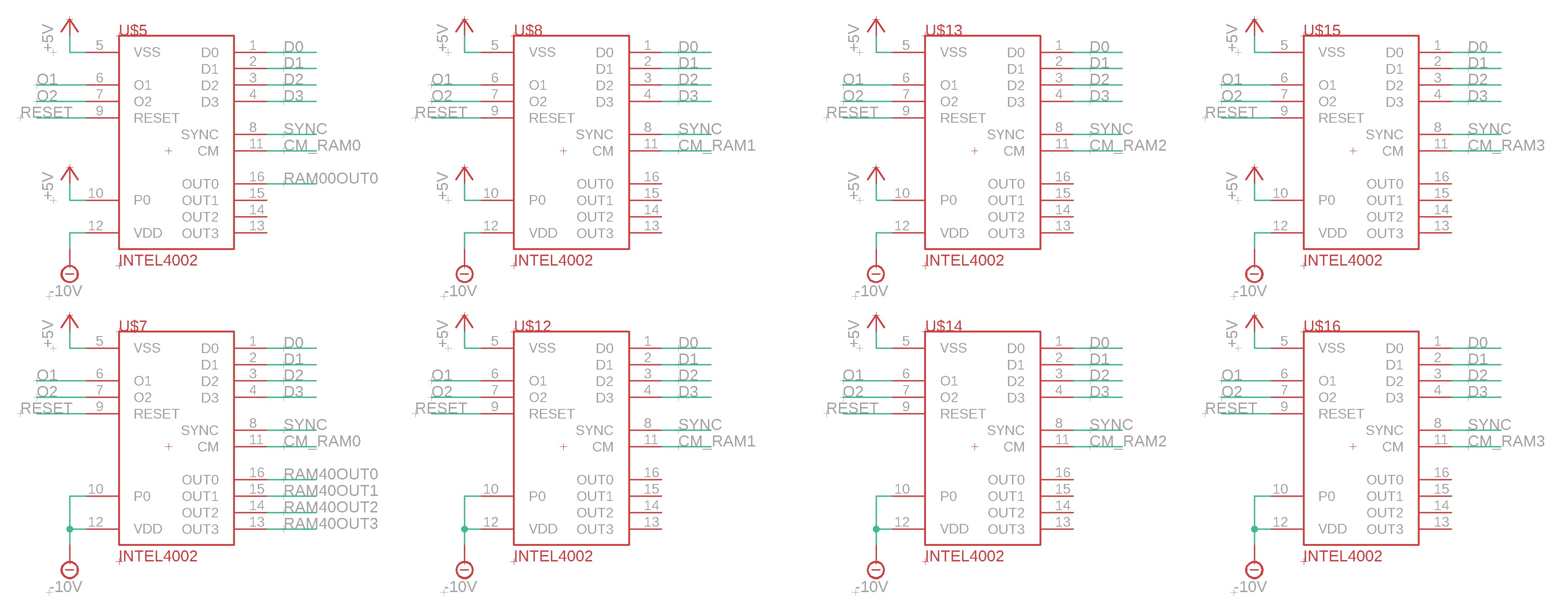
For the RAM, we’re going to use 4002-1 RAM chips. These each have 320 bits of storage. Yes, I said “bits” not bytes. It’s not a lot of RAM. You don’t have to add them in pairs, but it’s easy to do them in pairs by tying the P0 high for one chip and the P0 low for the other chip. You can then do four sets of pairs, for a total of up to 8 RAM chips. Note that you can’t share a pair with the 4265 if the 4265 is operating in mode #12 as it will use up all the RAM addresses. So the fourth (CM_RAM3) pair on my board pretty much has to sit empty. We have one thing left to show, and that is the multimodule interface:
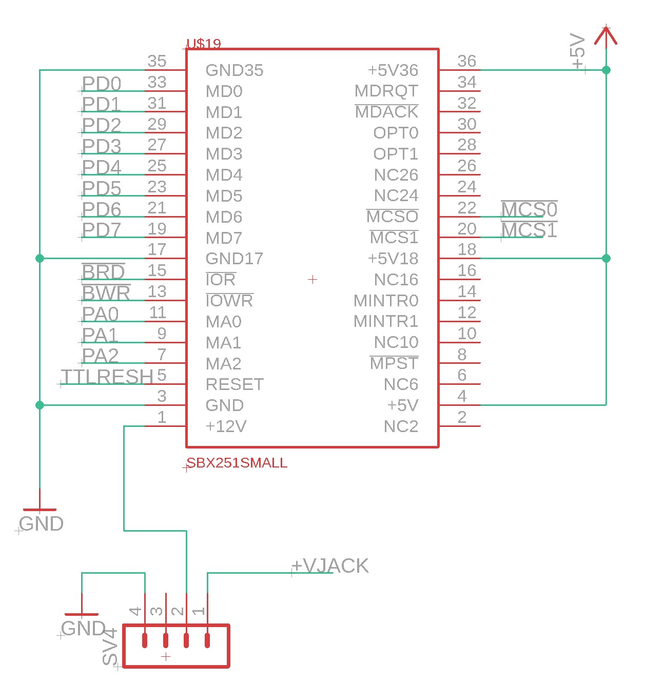
Multimodules became popular a few years later, in the 8080 multibus era. I’ve been doing a lot with multibus lately, and I have a pile of multimodules that I’ve designed. Multimodules use a 36-pin socket in a piggyback configuration. So I added one such socket. It’s interfaced just like the RC2014 bus, with the 4265 operating the address bus, data bus, and read/write strobes. The two chip selects (MCS0 and MCS1) come from the 74HCT138 on the first page.
There you have it. 7 pages of schematics. A lot of “optional” features.
Implementation
I had a pcboard fabricated:
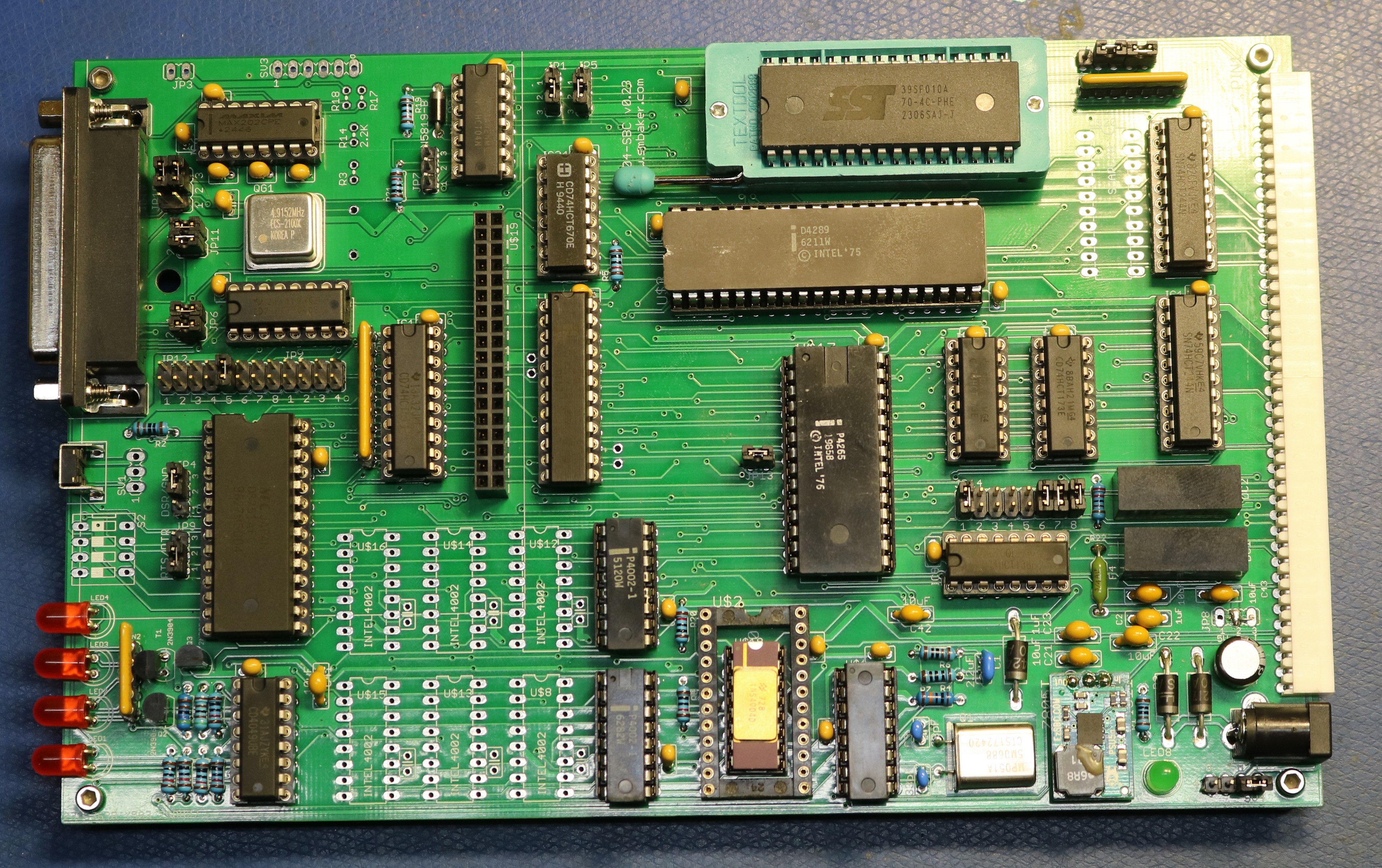
I don’t think there’s a whole lot to say here — I pretty much explained it all when discussing the schematics. The gold IC is the 4004. It’s installed in a 16-pin socket, which is surrounded by a 24-pin socket, so you can remove the 16-pin 4004 and install a 24-pin 4040 if that is your wish. The 4040 is certainly a lot less expensive.
The big white socket on the far right is a female 0.100 connector for the RC-2014 bus. The 2×18 socket in the center-left is the multimodule connector.
The big ZIF socket is for the ROM, and right below it is the 4289. Below the 4289 is the 4265.
Scott,
I watched your video on running Zork on the i4004. Impressive work! At the end of the video you explained that you printed the scores in hexadecimal because of the difficulties of converting to decimal. If it helps, I’ve added a function to print a 16 bit number as decimal to my Github repository: at ‘https://github.com/jim11662418/Intel_4004_Single_Board_Computer’
Cheers – Jim Loos
Thanks Jim, that doesn’t look so bad at all! I’ll see if I can incorporate it. Scott.