I always wanted to build a single board “trainer style” computer:
Motivation
When I was first getting started with electronics, wanted a Heathkit ET-3400 Microproccessor trainer, but could never afford one at the time. Eventually both I and the world moved on, to fancier more capable computers. However, I’ve still always wished I had an iconic trainer, complete with LED displays and a hexadecimal keypad. So I decided to build something of my own.
Note
Gerbers are finally released! People have been asking for these boards for a few years, and honestly I did at one point consider moving into the pcboard sales business. 🙂 But, as usual I’ve procrastinated. So to all those who are looking for boards, you can now download the gerbers yourself, submit them to JLCPCB, and have boards manufactured. Cost for 5 boards at JLCPCB is typically around $50 + shipping. Find them at https://github.com/sbelectronics/z80sbc.
A brief feature list
- Z80 CPU
- RC-2014 Compatible Expansion Connector
- Eight TIL311 Displays, or a 2×16 LCD/VFD Module
- 20-Key Keypad for cherry MX Blue Keyswitches
- Two serial ports (Z80 SIO/2)
- 24-bit Parallel IO Connector (Z80 PIO)
- Counter/Timer chip, optionally usable as a baud rate generator for the SIO/2
- 512 KB of banked RAM
- 512 KB of banked ROM
- Single stepper, with automated slow stepping feature
- Flexible IO address decoding using programmable logic devices
Design
The schematic is too big to inline into this blog post, it’s a solid 6 pages long. As such I’ve included a PDF link:
The schematic is divided into pages, each page serving a logic block of functionality
Sheet 1: Display and Keypad
There are two display options, TIL311 LED displays or a 2xz16 LCD/VFD. I really like the TIL311 display and have used it in several of my projects. It features a built-in 4-bit hex digit decoded, so you can simply write four bits to the display and the appropriate character shows up. There is an optional blanking input that lets you turn off the display, and inputs for decimal points. The problem with the TIL311 is that it is not currently manufactured — you have to find them on eBay. It’s also a bit of a power hog.
Data bus to the TIL311 is buffered via a 74HCT244, otherwise eight of these displays would quickly load down the Z80 Bus. Blanking inputs are latched by a 74HCT374. The left-hand decimal points are also latched by another 74HCT374. I chose not to implement the right-handle decimal points.
As an alternative to the TIL311, I provided a header to connect a parallel 2×16 LCD (or VFD) display.
The keypad uses Cherry MX Blue keyswitches. There are 20 keyswitches, and they are served by a set of three 74HCT244. There are ways to implement a keypad with fewer chips using strobing approaches, but using the 244 ICs allows for a simple one key = one data bit approach. Three 74HCT244 provide 24 bits of digital IO and we only have 20 keys, so I ran the remaining 4 bits to a dip switch.
Sheet 2: CPU and Expansion Header
This sheet is pretty straightforward, it’s just the Z80 CPU and the RC2014 expansion header, which features most of the pins of the Z80 CPU. Several of the pins on the RC2014 are “optional” and are brought out to jumpers. These include TX and RX from the SIO/2. bus control signals like BUSRQ, BUSAK, HALT, and WAIT.
There’s an RC power-on reset circuit, a crystal oscillator (connect the jumper JP3 to enable it), a 3-terminal regulator (I suggest using an EZSBC drop-in switching replacement for the 7805), and some blinky LEDs tied to some of the bus signals.
Sheet 3: Memory
Both the FLASH and the RAM are on this sheet. Memory paging is implemented using some 74HCT670 register files, see my paged memory board for the RC2014 for a description of how the memory paging works. The paging design is borrowed from Sergey Kiselev’s Zeta-2 single board computer.
The FLASH chip is brought out to an extra large footprint that allows installation of a ZIF socket. The ZIF socket is useful if you plan on reprogramming the FLASH more than a handful of times, such as if you wish to develop a custom CP/M distribution.
You’ll need to program the FLASH chip, a 39SF040. I recommend using one of the TL866 variant of USB Eprom programmers widely available on eBay.
Sheet 4: IO Address Decoding
I went a different route than my usual design here. Typically I would use some 74HCT138 3-8 decoders and headers to select which addresses to assign the onboard peripherals. However, we’re talking a lot of peripherals. I really wanted the peripheral addresses to be configurable, but without taking a lot of board space. My choice was to use ATF16V8 programmable logic devices.
The ATF16V8 can be configured with 10 inputs and 8 outputs and internally is implemented with a bunch of fuses that let you program logic between the inputs and outputs. Implementing address decoding is a relative piece of cake. I was able to squeeze in seven address bits and a write line into one of the ATF16V8 and seven address bits and a read line into the second ATF16V8. This lets us put write-only peripherals on the first chip and read-only peripherals on the second. Read/write peripherals can be placed on either.
The programming for the ATF16V8s is located in my github repo. For those wanting the standard board, you should be able to use my fuse maps directly. For those wanting to assign different addresses, for whatever reason, you can write your own fuse maps. I have some helper utilities to build the fuse maps. Most people will just use my fuse maps. You can often use the same EPROM/FLASH programmer that you’d use for the 39SF040 FLASH chip in the memory sheet to program the ATF16V8 chips.
Sheet 5: Serial, Parallel, and Counter/Timer
In this sheet, we have our input/output peripherals. The SIO/2 chip is our serial chip and gives you two serial ports. For running CP/M, you’ll end up using one of these ports as your console. The other port you can use for whatever you want (I connected a serial GPS for my Z80 Nixie Clock project). The first serial port is brought out to both a DB9 via a MAX232 serial driver chip and to a header that’s set of typical FTDI TTL-serial-USB cables. Personally I think the DB9 is cool, because that’s what a retro computer would have used.
The PIO chip provides 24 bits of parallel IO all brought out to a header. You can use it to drive LEDs (with an appropriate dropping resistor), read switches, interface with external peripherals, whatever.
The CTC is a counter-timer chip. It has several internally counters/timers that can be used to pulse its outputs at a specific rate. The primary use of the CTC would be as a baud rate generator for the SIO/2, if for example you wanted to be able to support both a 115200 baud console and a 9600 baud GPS.
Sheet 6: Single-Stepper
Sheet 6 is my single stepper, copied verbatim from my RC2014 single-stepper page. Check smbaker.com or my videos for a detailed description [TODO: dig up the links].
The single-stepper allows you to step through a program one instruction at a time. Why would you want to do this? If you were using this as an actual trainer, programming directly in assembly language, then it could be handy. In addition to single-stepping, it also supports a mode that I called “slow-stepping” where a 555 timer automatically pushes the “step” button for you. This makes a program run really slow. Like in the tens or hundreds of instructions per second rather than millions.
Implementation
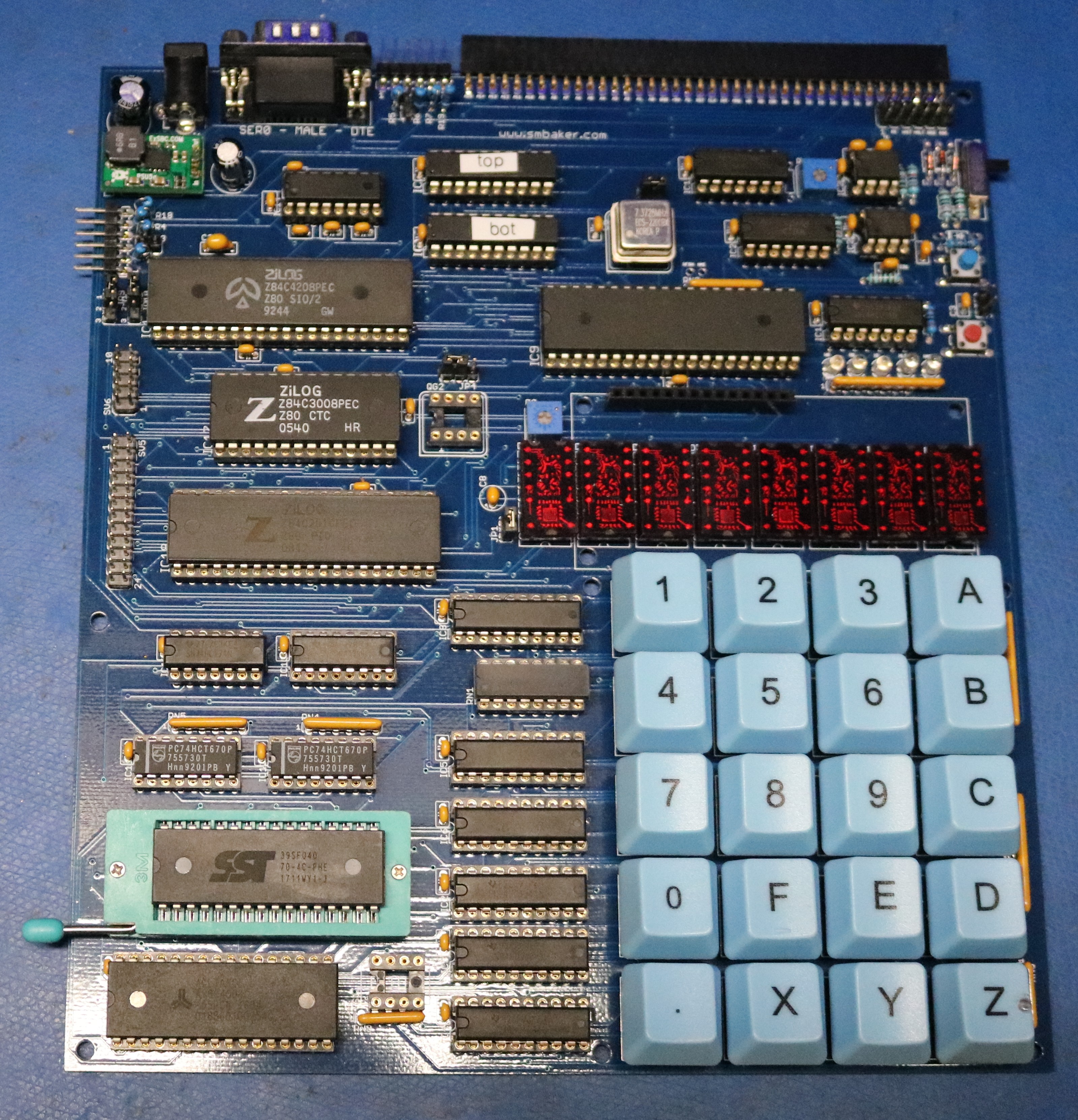
Okay, so it’s been years since I did this and wrote this blog post, with a “TO-DO” comment here. I was going to talk about all the steps necessary to make yourself a wonderful 4-layer PCBOARD. The best comment I have is to watch the video and hope I explained it all there. Below is a high-resolution (click to get more detail) picture of my completed board.
Initial configuration
This section describes how I set the crystals, jumpers, etc on my board.
- IC7 (rearmost PLD) is programmed with PLD file z80sbc-1.pld which is compiled into the jed file z80sbc-1.jed. (note the “name” set in this file says z80sbc-2. oops. Use the filename to know which is which)
- IC16 (frontmost PLD) is programmed with PLD file z80sbc-2.pld which is compiled into the jed file z80sbc-2.jed
- Diode D1-OPT (between single-step button and slide switch) is not installed.
- QG1. Primary oscillator. 7.3728 MHz.
- QG2. Serial oscillator. Not installed (use JP4 in positions 2-3)
- JP1. TIL311 power. Jumper installed.
- JP2. Primary clock. Jumper installed.
- JP4. SIO and CTC clock source. Set to positions 2-3 to use OG1 as the serial clock.
- JP9. RX clock source. Set positions 1-2 to use SCLK, which is derived from JP4.
- JP10. TX clock source. Set positions 1-2 to use SCLK, which is derived from JP4.
Initial power up
Power the board up with the slide switch in the rearmost position. The board doesn’t necessarily always reset properly, so I suggest pressing the reset button to be sure. The reset button is the button closest to the six LEDs.
Observe the LEDs. You should see WR and RD lit fairly steadily. If you look closely enough, you may be able to discern some blinking in the IO LED, though it is very infrequent.
If you move the slide switch all the way forward, you may be able to see WR and RD blink more slowly. Put the slide switch reward and reset again.
If you want to poke around with your oscilloscope, you can check the following when the computer is idle:
- IC7 (rearmost PLD) pin 11. M1. Should be steadily pulsing, one pulse is each instruction fetch cycle.
- IC7 (rearmost PLD) pin 1. IOREQ. Should pulse twice every 1.3ms.
- IC7 (rearmost PLD) pin 2. WR. Blinks a lot.
- IC16 (frontmonst PLD) pin 11. M1. Same as IC7 pin 11. Should be steadily pulsing, one pulse is each instruction fetch cycle.
- IC16 (frontmost PLD) pin 1. IOREQ. Same as IC7 pin 1. Should pulse twice every 1.3ms.
- IC16 (frontmost PLD) pin 15. SIO Chip Select. Should pulse once every 1.3ms.
Now it’s time to check the serial port. Assume IC11, the MAX202, is installed. You can connect your 9-pin serial cable, probably with a null-modem adapter, to the DB9 jack. Set your terminal to 115,200 baud. Press the reset button and you should see the CP/M banner.
Alternatively, you can plug a USB-TTL 5-pin cable into the 5-pin header on the side (between the voltage regulator and the SIO chip). Do this with the MAX202 REMOVED. Setting your terminal to 115,200 baud, and pressing reset, you should see the CP/M banner.
Note that the TIL311 displays do not light up. If memory serves, I wrote a few demo programs to use them, but I build nothing into the CP/M OS itself.
Github resources:
- https://github.com/sbelectronics/z80sbc, Scott’s Z80SBC repository containing schematics, code for the
- https://github.com/sbelectronics/RomWBW, my fork of the RomWBW CP/M distribution.
A great project. I’m Interested in buying a z80 sbc pcb. Thanks.
Hi Scott,
I am not sure my earlier message reached you so I try again. I would love to build your SBC and I wonder if you still have one PCB available.
Hope to hear from you soon.
Kind ragards,
Peter
peter@vdbg.nl
Hello Peter, I do have boards, but don’t have any shipping materials for them right now for such a large PCB. I suppose I should look into getting some larger boxes.
Hello Scott,
I am interested in building your board. Do you still have any boards available? I have not looked yet, but do you have a bill of materials for the required parts? Could you give an idea on what the parts cost should be? Did you source your parts from the PCB board companies sister company that does parts?
As you can see, while I would love to build one, I am in the price and BOM availability and feasibility stage at the moment.
Thanks for your time!
Brian Boothroyd
Great stuff.
I was also wondering if you have an SBC available.
Best regards,
Diego
Very Interesting! followed your RC2014 series. Excellent. purchased the RC2014 kit from Spencer. 😉
But having trouble with serial I/O. :-]
notice the RC2014 header : I could use something to help with trouble shooting modules. ??
not giving up on the Z80 stuff. too close to understand what needs to happen. 🙂
would like your board if you decide to sell some.
Verl
I’ve built up the RC2014 and a few modules. VFD, bus monitor, RTC. This SBC is great. I’d be very interested in a board along with a BOM, if available.
Hello Scott,
What would it cost me to get you to send me one of these boards. I will mail you shipping materials if necessary.
Chris
Hi Scottie like to buy one of your z80 4 layer rc2014 compatible PCBs please.
I live in the UK
Regards
Kim
I think this project is abandoned. The board is lost to history.
If you have any PCB’s still I would love to puchease one or two of them.
Any chance on doing another run? i would be willing to pay to cost of JLPCB doing five boards and for your time… If willing you could upload the files to jlpcb and have it drop shipped to me 🙂 pretty please 🙂
Scott, I would love to order two of these PCBs. Is that possible?
Hi:
Wow what a NICE trainer!!
Do you have any PCB’s for this trainer for sale?
If so, how much are they?
Thanks,
Ron
n6idlron@comcast.net
Scott ,
Where did you get those key caps ? I have been looking for MX blue key caps with centered numbers and letters forever.
Can you tell me your source ?
They came from WASD Keyboard, https://www.wasdkeyboards.com/. There’s a template where you can drop your own graphics on the keycaps, any way you want to do it using Inkscape.
I’m not really interested in selling boards at this time, as packaging them up for safe travel in the USPS takes a bit of work. I have, however, made the gerbers available in the github repo, so people can submit an order to JLCPCB and have the boards directly shipped to you!
Cool project! Ordered boards this morning from JLCPCB for the SBC. Your SBC is so awesome because of all the cool features. I used an Intel 8085 sbc in a technical school many years ago that was really limited.
I’m just getting into the RC2014 retro computer scene, I ordered boards for the Bus Monitor and Stepper.
Thanks for the keycaps information, I had no idea you could order custom keycaps. Really helps when building projects to let us know vendors.
I really appreciate you taking the time to do blogs for your projects. It takes a lot of time.
Thanks again, Jerry
Awesome, please let me know how it turns out!
JLCPCB just sent me an email this morning with a problem with the z80SBC PC Board.
JLCPCB email content:
Sorry to bother you, but there is an issue that we want to confirm with you before proceeding.
As shown below, please kindly inform us your layer sequence .
z80sbc.cmp
z80sbc.crc
z80sbc.crs
z80sbc.drd
z80sb.cdri
z80sbc.gpi
z80sbc.l15 This one is highlighted
z80sbc.ly2 This one is highlighted
z80sbc.plc
z80sbc.pls
z80sbc.sol
z80sbc.stc
z80sbc.sts
Any idea what she is asking?
Thanks,
Jerry
I think she wants to know the ordering of the layers — since there’s two middle layers, which one is closer to the component side and which one is closer to the solder side. Rewatching my video (it’s the only way I can remember these things) it looks like this is how it is laid out from top to bottom:
CMP – component side
LY2 – topmost inner layer
LY15 – bottommost inner layer
SOL – solder side
Hi Scott, I got the pcb and loaded the components. The board boots up and will run c/pm, but my displays are blank. Checking out IC7 with my scope I get all the information on the inputs, OE line has alot of activity, but nothing on the outputs. I should be seeing the led latch strobes. I burnt another IC7 with z80sbc-1.jed. Still nothing, any ideas? Could the jed file be bad? I’m using the right JED file for IC7? Thanks, Jerry
Jerry, z80sbc-1 does look like the right one to go with IC7. What does your code look like for writing to the displays?
Hi Scott, Thanks for the reply. I tried verifying the z80sbc-1 and it wouldn’t verify. So I burned another and its working(the HTIL311A). Its interesting in your video, your displays turn on when powering up, mine dont display until I run your counter.bas.
I have one more problem, keys not working when running counter.bas. I put the scope on pin 19 of the z80sbc-2, I’m getting low pulses. What value of resistors array did you use for pullups on the keys? I believe I used some 10K I had laying around.
I’ll do some more troubleshooting later today.
Thanks for your help,
Jerry
Some idiot was so excited to start using the Z80sbc that they overlooked soldering the pullup resistors for the keys. They were installed with one pin soldered to hold it in place.
Keys are working now! Woo hoo!
Thanks,
Jerry
Thankyou so much for adding the gerbers. Soon I will have some of this board printed.
Hello Scott,
In the schematics, some component values are missing. I’ve made a BOM in Excel that shows the blanks. (Couldn’t find a mail address to send it to)
Components R11, RN 3,6,7,8,9 and SV3-4. Also frequency for OG1 and OG2.
Of course I can send the BOM and also add Mouser part numbers if you like.
BR/
Guus Assmann
Guus
could you email your BOM please….
Thank you
Mike Johnson