Although it seemed to work fine when I first built it, lately I’ve been experiencing some problems with my Xi 8088. The computer is fairly stable with 5 expansion cards installed (compactflash, CPU, OPL 2 (Adlib), Floppy, and VGA. However, it becomes significantly less stable as a sixth and seventh expansion card is installed. This post will document a few of the troubleshooting steps I have taken.
There’s a long-running thread over at Vogons, from a couple users who are also having issues. I’ve been using Checkit 3.0’s memory test as a means to diagnose the issue.
First of all, I started by trying to characterize the problem I was seeing. I switched Turbo mode off, so I was operating at the standard 4.77 Mhz. I started with my 5 card configuration and then added cards one at a time to gauge the affect on stability. The two additional cards I’ve been testing are an 8255 board (see my Xi 8088 Nixie Tube Clock post) and a CP/M Z80 “UNIDos” coprocessor. The 8255 board is relatively modern, using CMOS chips. The Z80 coprocessor is ancient with lots of LS logic. The 8255 board caused a small but noticeable degradation of stability. The Z80 coprocessor had a significant degredation of stability.
The first thing that came to my mind is bus loading. If adding additional ICs to a bus is causing instability, then it may be because the source and sink capability of some IC attached to that bus is not capable of driving the additional loads. A noisy bus could be a contributor to a load problem.
Anyhow, I started by first taking some measurements with my oscilloscope. The first picture is a baseline showing the 5V voltage signal:
This is around a volt of noise. While at first that seems alarming, I’m not convinced it’s real power-supply noise. It could just be common-mode noise between the computer and scope. I need to investigate this in more detail, as it wouldn’t be the first time I spent weeks tracking down a problem, only to realize it was a noisy power supply.
Anyhow, on to a more interesting graph. This one shows four lines on the ISA bus. Yellow = MEMR, Turqoise = CLK, Purple = A0, Blue = D0.
The baseline noise we measured above is present in all of the lines, making it a little bit hard to read, but we can see some interesting things. For example, there’s a huge overshoot and undershoot on the MEMR line. The clock line is ringing. There looks to be some undershoot and overshoot on the A0 line.
Note that a memory read occurs on a high-to-low transition of MEMR, so what we see above is the CPU setting up the address bits (purple trace goes high to indicate a 1 on A0), then MEMR goes from high to low, and finally the RAM responds, with a 1 on D0. At the end of the memory read cycle, MEMR goes high, and then the address bus is cleared. The data bus goes high-impedance, and D0 remains high because there’s nothing to pull it low.
Passive ISA Bus Termination
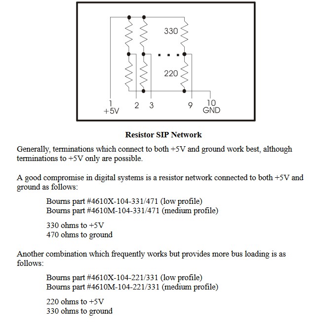
My first thought was let’s try to do something about the overshoot and undershoot on MEMR. I decided to construct a bus terminator board, using a 220/300 resistor network. The idea came from a backplane manual that I found online.
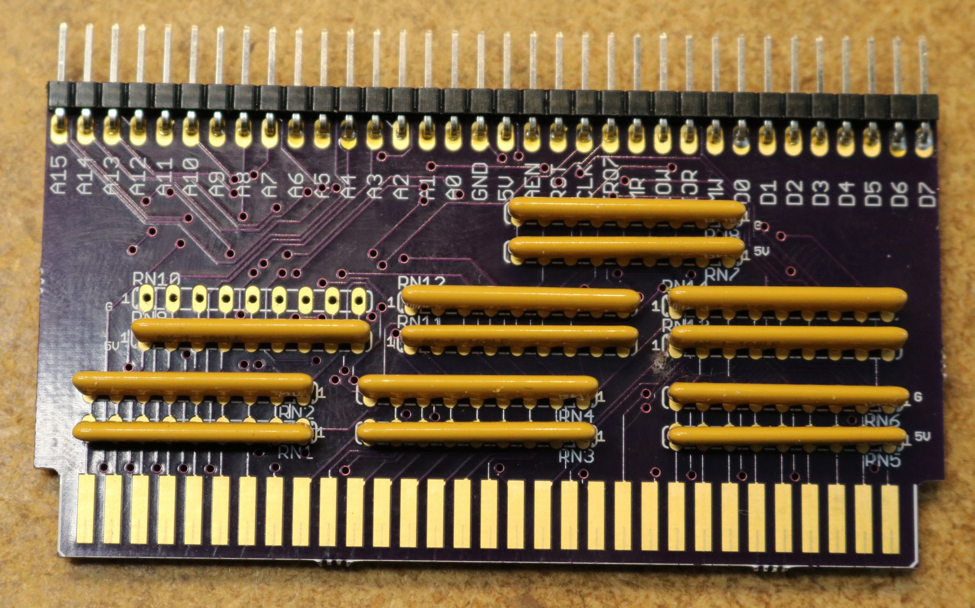
The 330/220 divider shown in the picture will pull signals toward approximately 2V. This is backwards from the 220/330 divider described in the text, which will pull signals toward 3V. In either case, it’s going to add some loading to the bus and additional power consumption. I opted to start off lightly and chose a 1K/670 voltage diver. I designed a board in Eagle and had it fabbed at Osh Park:
You’ll notice I left one of the resistor packs off, I’ve found that messing with IRQ6 will cause the Xi 8088 to hang during boot sequence with a Post code 06, right after playing the boot music. Haven’t taken the time to investigate why yet. Anyhow, let’s look at the scope:
Okay, there’s some improvement here. The overshoot and undershoot on the MEMR signal is gone. The clock is still ringing, though perhaps not as bad as before. The A0 pin is cleaned up. But, what’s happening with D0? It looks kinda wonky. Let’s zoom out on the signal:
Now it becomes clear what’s going on with D0. When there’s not an active data transfer, the data bus goes “high-impedance” — it’s neither pulled high nor pulled low by logic. My terminator board pulls it toward 2V. So what we’ve ended up with a sort of tri-state behavior on that data bus — high, low, and middle. There’s some slope as it transitions to high-impedance state, as there must be some capacitance in the system and that capacitance plus the terminator resistor is leading to a little RC circuit behavior. We’d get steeper transitions with lower value resistors.
The effect of this board on my Xi 8088 was noteworthy improvement at 4.77 Mhz, but still not perfection. Whereas an unterminated bus with seven cards installed would last 20 minutes on average before throwing a memory error, the terminated bus would last several hours.
Active ISA Bus Termination
Next I decided to try an active termination approach. Active termination for S100 boards is described here. The idea is that we regulate a voltage to approximately 2.7 volts, and then tie that regulated voltage to our various bus signals using a suitable resistor. I gave this a shot using 330 ohm resistors and my bench-top supply. The result was very promising, effectively fixing the stability issues when operating at 4.77 Mhz. It ran all night in the seven card configuration several times without failure. When operating at 8 Mhz Turbo speed though, I still had stability issues. So something is clearly still wrong.
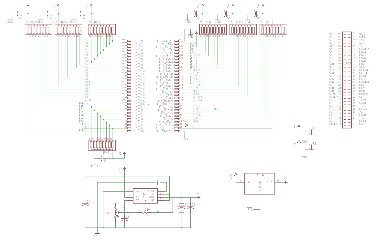
I designed a new board and had it fabricated at Osh Park. Here is the schematic:
As we can see above, there’s two separate voltage regulators, an LT1086 and an LT1118. Populate one or the other not both. To repeat, populate the LT1086 or the LT1118, not both!
I chose to use the LT1118 as it’s both a source and a sink regulator. The LT1086 is only a source regulator. I chose to use the LT1118 as it seems like being able to both source and sink current is an advantage for a terminator bus. Sourcing is necessary to pull signals up, and sinking is necessary to pull signals down. Whether the overall buss needs to be pulled up or down depends on the signal characteristics at the time. If you’re reading memory address 0xFFFFF, then there’s going to be a lot of highs on the bus. If you’re reading memory address 0x00000 then there’s going to be a lot of lows.
The regulator section is a pretty standard schematic of an adjustable voltage regulator. There’s a trimmer potentiometer that set’s the voltage. I set mine to about 2.7 volts. There are input (C1) and output (C9) filtering capacitor, I chose my values according to the LT1118 data sheet at 1.0 uF each. Capacitors C10 and C11 I did not populate. I suggest doing a rough setting of the voltage on the bench — hook up the board to a 5V supply, attach a multimeter to the VTERM line (pin 1 of JP1), and adjust the pot for 2.7 V.
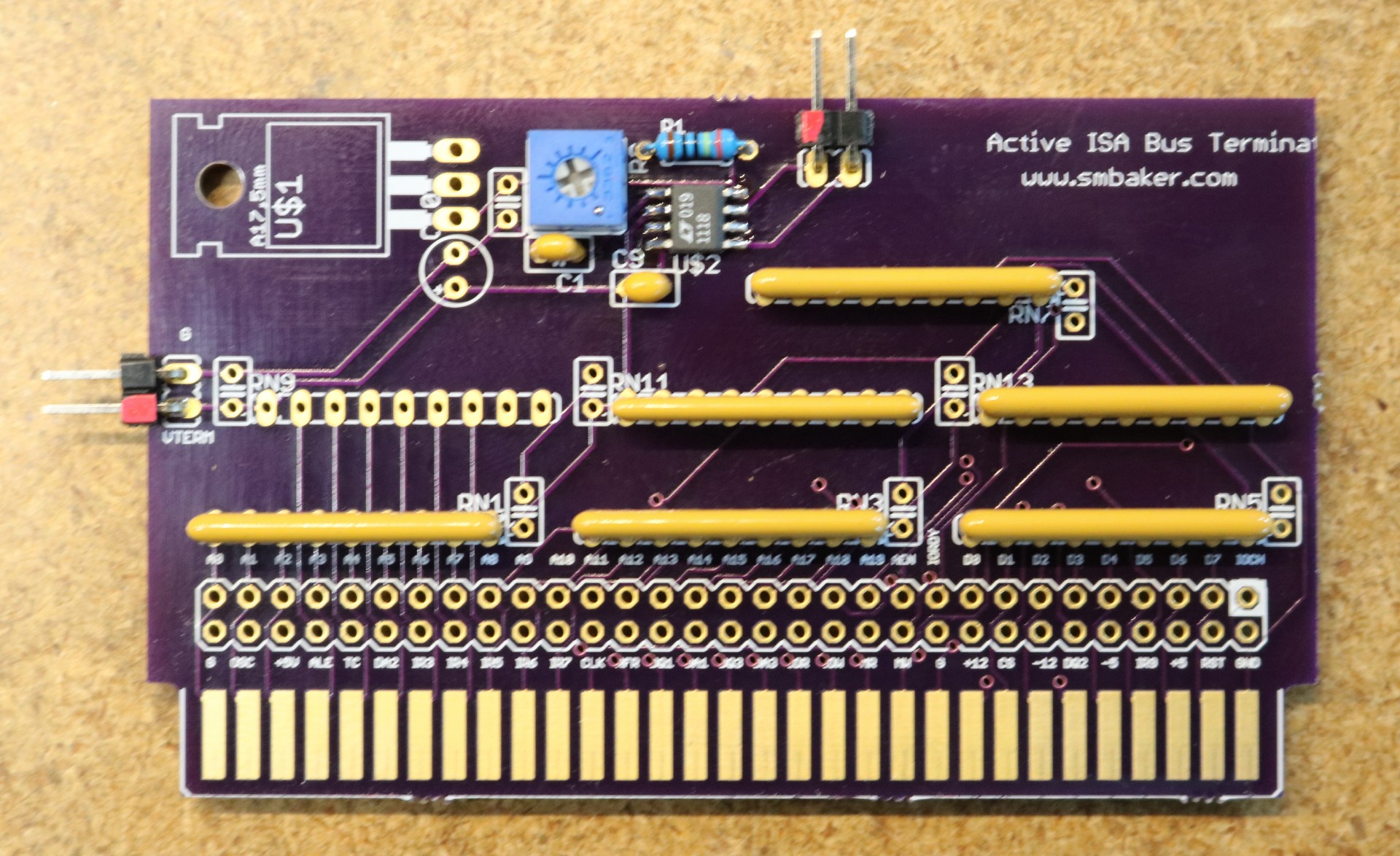
There are seven resistor packs that are are attach various bus lines to the termination voltage. I did not populate RN9, as RN9has that troublesome IRQ6 on it, that tends to cause my computer to not boot when I mess with it. Your mileage may vary — it may make sense to slowly apply resistor packs starting with the address (RN1, RN3, RN7) and data (RN5) buses, and then the control buses (RN11, RN13)… or maybe you just want to do what I did and populate everything except RN9. The value of resistor is up to you. I chose to use 220 ohm. You might be able to go lower than that, but be wary of the current limit of the LT1118, which claims to be able to terminate “27 SCSI lines” at 110 ohms. I figured up to 56 ISA lines at 220 ohms out to be about right. Below is a picture of my completed board:
As a reminder, note that I populated only one of the regulators, the LT1118. Also note the two capacitors I installed, those are 1 uF each. Finally, pay particular attention to the orientation of the LT1118. The “slanted side” is to the right, and pin 1 is installed toward the bottom. For some reason, silk screen showing IC orientation didn’t make it onto the board. Also note that RN9 is unpopulated. The header at the top of the board is 5V and GND, the header at the side is Vterm and GND. There’s provision to install additional filtering capacitors (I suggest 0.1 uF) at each resistor pack. There’s provision for you to install a dual-row header at the bottom of the board — this could be used for attaching scope probes or other diagnostic tools. I chose to use a single-turn 5K potentiometer. A 10-turn potentiometer might make for better fine adjusting.
Test results of the active bus terminator have proven very promising. I’ve had it run all night long with Checkit, at Turbo speed. I’ve left it running for hours running a game demo.
RAM Selection
The other place that we could be going wrong is with the RAM. The Xi 8088’s memory system is not buffered. The AS6C4008 Static RAM chips are attached directly to the ISA bus. While the logic chosen in the Xi 8088 design, primarily 74F and 74ALS ICs, has plenty of source and sink capability, the capability of the SRAM chips is unknown. The datasheet specifies a output high and output low voltage at a given load (high = 2.4V at -1ma, low = 0.4V at 2ma), but doesn’t specify a maximum load. Some experimentation would be necessary to generate a curve of output voltage versus output current.
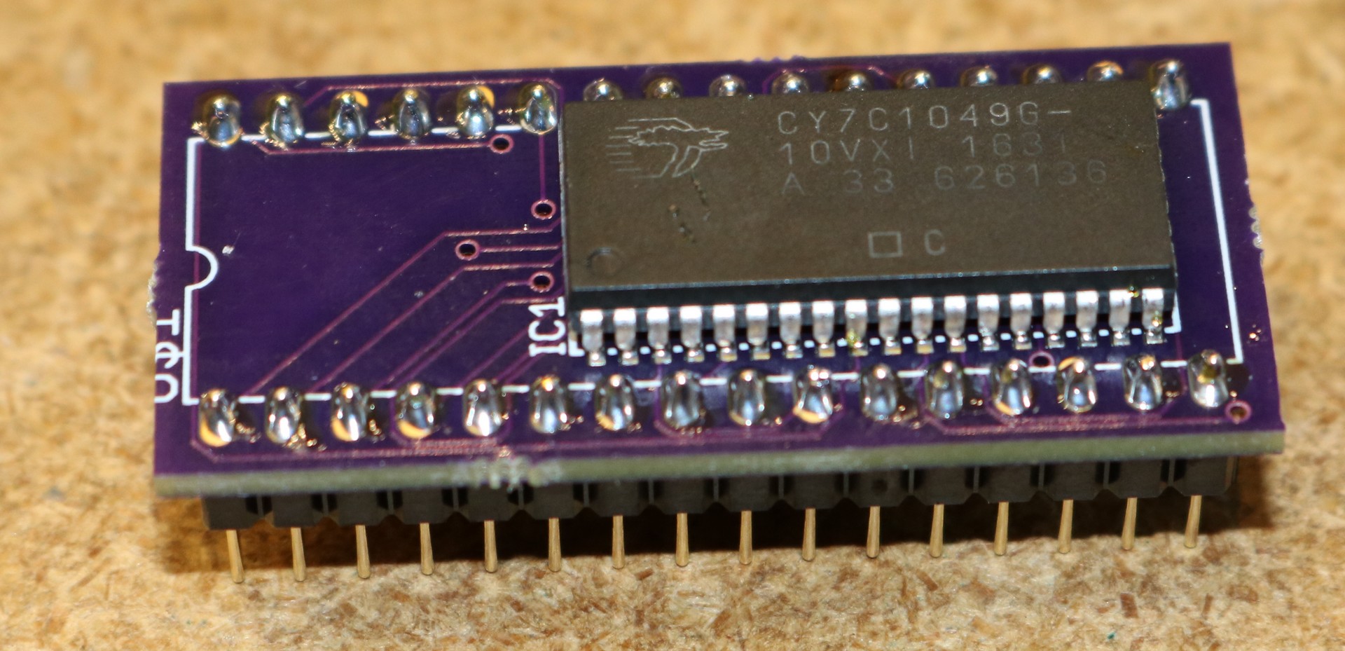
The first thing I thought I would try is substituting a different Static RAM chip. The CY7C1049G datasheet specifies high of 2.4V at -4ma and low of 0.4V at 8ma. That’s four times the published specification of the AS6C4008. That doesn’t necessarily mean that the IC is capable of sourcing and sinking four times as much, but rather that those parameters are what the engineers tested. The CY7C1049G is also considerably faster (10ns vs 55ns) and has on-board ECC. Seems like a good choice. Unfortunately, it’s available only in SMD, so I built myself a breakout board:
I tried this out, without my bus terminator board, so I could evaluate the change in SRAM by itself. Unfortunately, switching SRAM didn’t help. Not one bit. If anything, it made the computer a little more unstable.
RAM Buffering
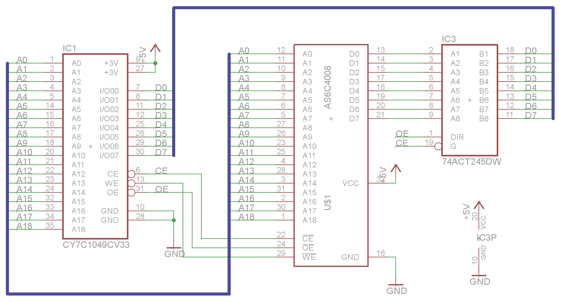
As I mentioned in the previous section, the Xi 8088’s Static RAM isn’t buffered. It’s attached directly to the ISA bus. The guys over in the Vogons thread had the idea that if I ought to add a buffer IC to my breakout board, and then we’d have fully buffered memory. It wouldn’t matter what the SRAM could source and sink. If we stick the SRAM behind a 74ACT245, then we’ll be able to source and sink 24ma.
I currently have a new set of breakout boards being fabbed at Osh Park, with onboard 74ACT245. Here’s the schematic:
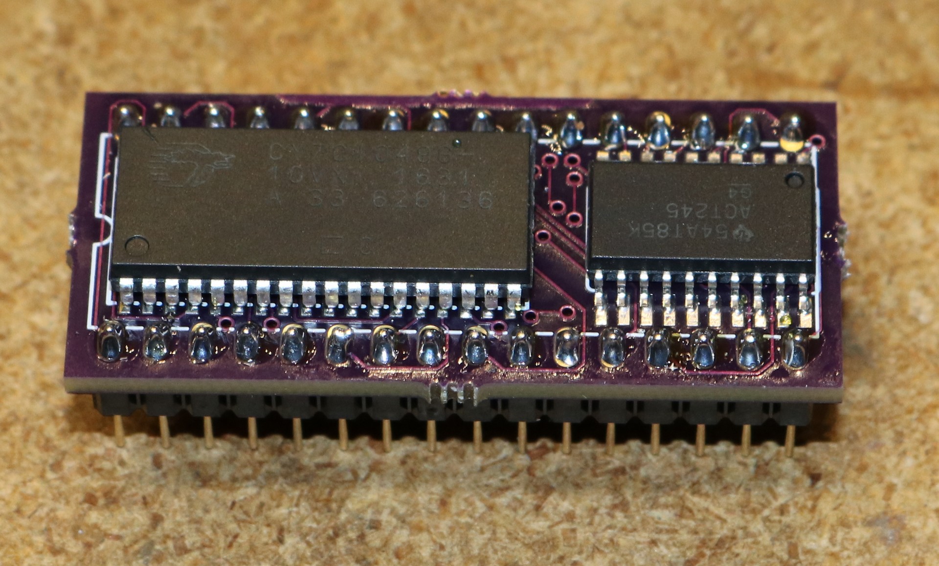
and a picture of my completed board:
Again, I tried this out, without my bus terminator, so that I could see if the change in SRAM made any difference. Unfortunately, the buffered memory board was not a success. It was far less stable than the unbuffered board, or the plain ordinary AS6C4008 DIP chips. My Xi 8088 would not boot with the buffered memory in the first position, and would only recognize 512K if I tried to place the buffered board in the second position, reporting a memory error. By pressing escape during the memory check, I was able to boot with the the buffered memory installed in the second place, but checkit confirmed there are a high rate of errors on the buffered memory.
This was really a surprising development. Sticking a 74ACT245 in front of the memory chip shouldn’t cause the memory system to become more unreliable. If anyone sees an obvious flaw in my approach, please let me know as I’m curious what went wrong.
Power supply filtering
I am using a Mini-Box PicoPSU power supply. A few of the reviewers of these mini-box power supplies have complained of power-supply instability. If the 5V line isn’t stable, then it could explain numerous stability problems with the PC. Nevertheless, I tried a standard ATX power supply, and the stability problems remained.
Another thing to look at is the bypassing. There’s lots of bypass capacitors on the Xi 8088 and on the backplane, but I did use ultra-cheap China eBay bypass capacitors. Maybe they’re just not good.
Conclusion
I tried several techniques for improving stability of my homebuilt 8088 PC. Trying different static RAM proved to be not helpful, and attempting to buffer the static RAM made stability much worse.
Where I did have success was with bus termination. The passive bus terminator showed a significant improvement in stability. It may have shown greater improvement had I been braver with my resistor selection. The active bus terminator showed massive improvement, perhaps fixing the stability problem altogether. My recommendation for anyone else who experiences stability issues on an ISA backplane is to try using an active ISA terminator.
PC-Board Ordering
If anyone is looking for the PCBs mentioned in this post, they’re available on osh park as usual:
 Active ISA terminator board (my conclusion showed this to be the recommended solution)




Did you happen to take some scope traces of the bus signals when using your active termination card? I’m very curious to see the performance of that solution compared to the passive solution.